Facebook
 Google
 GitHub
 Linkedin
Widlar’s Improved Bandgap References
It's Widlar's turn again. Four years after Brokaw described his voltage reference, he came up with a whole series of new bandgap reference designs. Figure 9-10 shows just one of them.
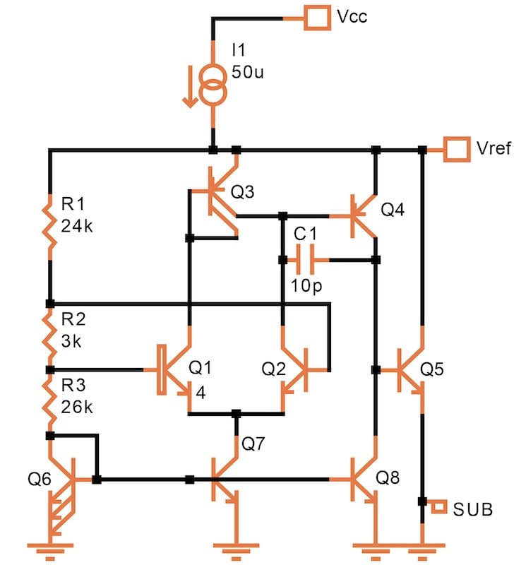
Figure 9-10. One of Widlar’s new bandgap references. [click to enlarge]
In this figure, the emitters of Q1 and Q2 are connected together. As a result, the ΔVBE shows up between their bases—in other words, across R2. The 4:1 ratio for Q1/Q2 was selected just for some variety. At room temperature and with this small ratio, we get:
$$\Delta V_{BE} = \text{ln}(4) \times 26 \text{mV} = 36~\text{mV}$$
Since there’s only one current flowing through all three resistors (ignoring the small base currents of Q1 and Q2), the total voltage drop across the resistors is 36 mV (53 kΩ/3 kΩ) = 636 mV.
Add the 600 mV VBE of the diode-connected Q6 to this, and you get a temperature-compensated reference voltage of 1.236 V. Note that this value and the required values for R1 or R3 may be somewhat different for other processes.
The multiplying resistor has been split into two parts (R1 and R3) to provide enough headroom for the transistors to operate. The operating currents for the differential stage (Q1, Q2) and the second stage (Q4) are reduced by making Q6 three times as large as Q7 and Q8.
This reference requires a minimum current of 25 μA to operate properly (Figure 9-11). Above that level, the impedance at the output is about 10 Ω. Frequency compensation is easily accomplished by enhancing the Miller capacitance of the slowest device (Q4) with a 10 pF capacitor.
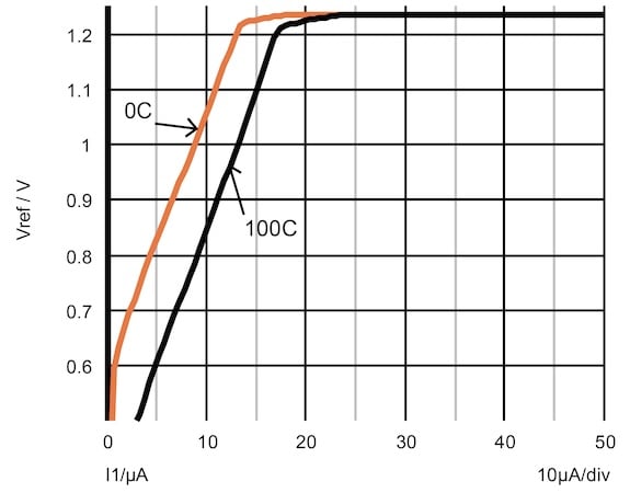
Figure 9-11. Minimum operating current of the improved Widlar bandgap reference.
Voltage Variation
Let's look at the variation again. Once either R1 or R3 is optimized for near-zero change at the temperature extremes, we get the inevitable bow (Figure 9-12). For this reference circuit, it amounts to 0.15%.
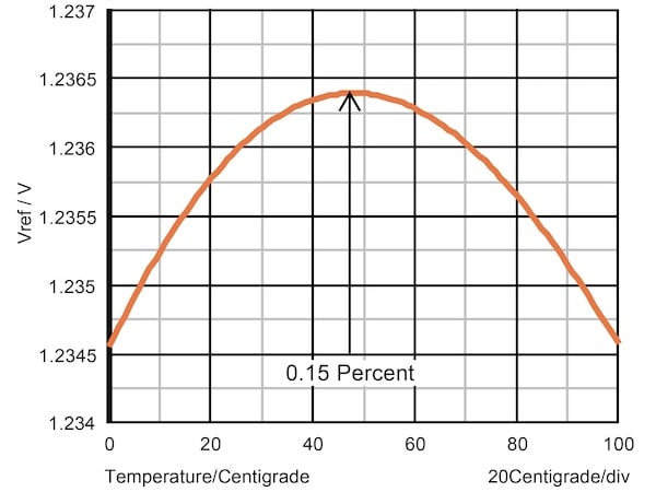
Figure 9-12. Output voltage deviation over temperature (the bow).
However, we also need to add the production variations due to the absolute value of the VBE and the matching variations of the resistors and transistors. When we run a Monte Carlo analysis of this circuit, we get quite a different picture (Figure 9-13).
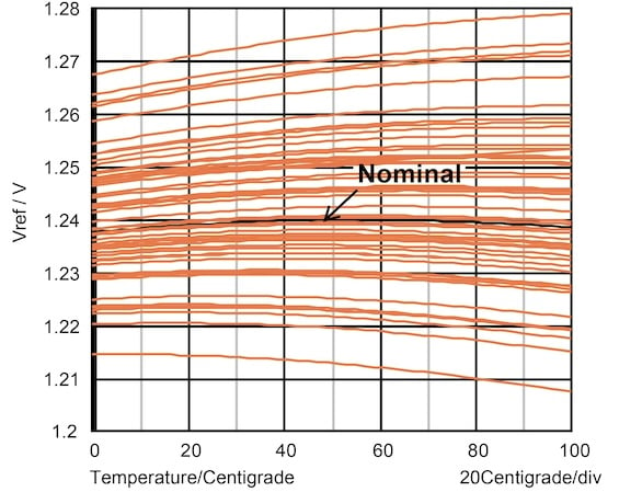
Figure 9-13. The voltage bow across temperature is a minor factor in the overall variation.
Here, the 0.15% bow is overwhelmed by the ± 3% overall variation. It’s worth noting, though, that the variation can be reduced to perhaps ± 2.3% by choosing a larger emitter ratio.
Second-Order Temperature Compensation
At the same time that Widlar introduced his new designs, he also came up with a way to reduce the bow, a method which is now called second-order temperature compensation. To illustrate, we’ll use the circuit in Figure 9-14.
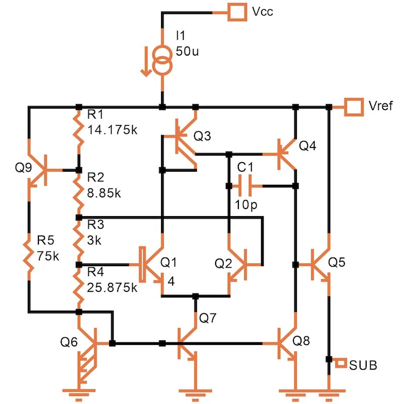
Figure 9-14. Bandgap reference with curvature correction. [click to enlarge]
This is the same bandgap reference circuit as Figure 9-10, with just one transistor added. A portion of the voltage across the resistor string is tapped by the base-emitter diode of Q9 with a large-value resistor. The tapped voltage has a positive temperature coefficient, and the base-emitter diode has a negative one.
At about 40 °C, Q9 and R5 start feeding a small current into Q6, which increases as the temperature is increased. This bends the right-hand side of the characteristic bow upward. R1, R2, and R4 then need to be adjusted to level the curve, a somewhat delicate process. The net result, after several adjustment cycles, is the flatter curve shown in Figure 9-15.
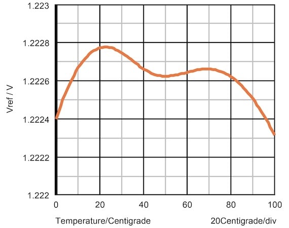
Figure 9-15. The bandgap reference voltage bow is reduced by second-order temperature compensation.
Figure 9-15 shows a deviation of just 0.04%. But let's put this in context again. We may have straightened the nominal curve, but—as we see in Figure 9-16—it’s still subject to the variations caused by VBE and matching. After accounting for these variations, we see little or no improvement in overall accuracy. The overall variation now overwhelms the remaining bow, so this approach should only be used with trimming
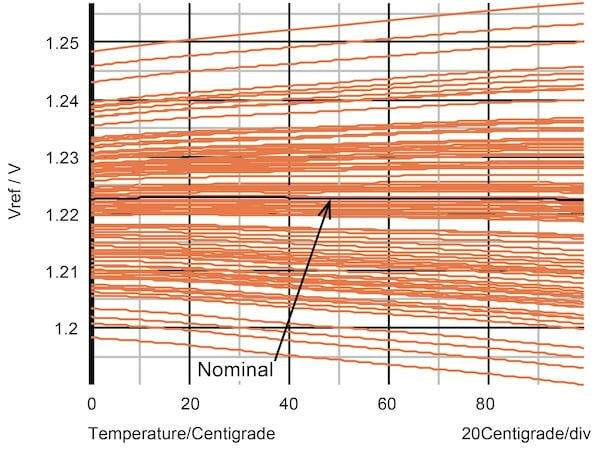
Figure 9-16. Monte Carlo analysis of the bandgap voltage reference with second-order temperature compensation.
An Advanced Bandgap Reference with 2·VBE Output
Figure 9-17 shows a more modern bandgap reference. It’s more accurate without trimming than the previous examples.
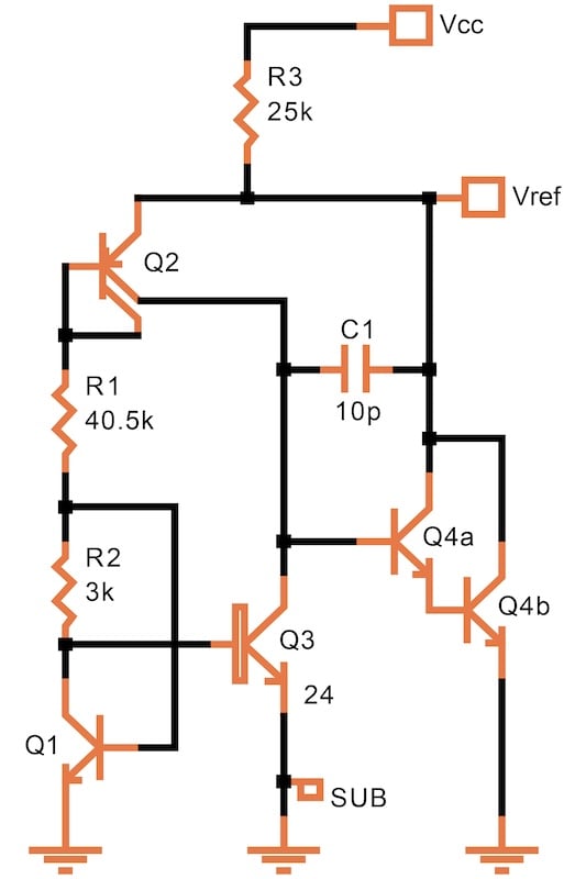
Figure 9-17. An advanced design for a 2.5 V bandgap reference. [click to enlarge]
It’s basically a two-terminal reference circuit fed by R3. Just four transistors are used, one with a dual base/emitter. There are two diodes connected in series, so the output voltage is twice the bandgap potential (2.45 V). With R3 = 25 kΩ, the optimum Vcc range is 4.5 V to 5.5 V.
The ΔVBE appears across R2. The 24:1 emitter ratio of Q3 to Q1 generates about 83 mV at room temperature and is multiplied by R1 to achieve about 1.2 V. The difference here is the placement of R2 in the collector circuit of Q1, which subtracts rather than adds the ΔVBE.
One VBE is that of the lateral (split-collector) PNP transistor Q2, and the other is from the NPN transistor Q1. Lateral PNP transistors generally have a narrower variation in VBE, but work only over a limited current range. The error signal is picked up by a Darlington pair transistor (Q4 in which there is one shared collector region and two base-emitter patterns.
Let’s look at a few of the details of this bandgap reference:
- Process variation: Variation in production over a temperature range of 0 to 100°C is a mere ± 1.6% for this circuit. As always, the values given here are for a specific process with fairly large dimensions (the resistors are 4 μm wide). You may need to adjust R1 for other processes and certainly will for other emitter ratios.
- Frequency stability: The circuit is stable with a load capacitance of less than 50 pF or greater than 200 nF.
- Power supply rejection: With a 330 nF capacitor at Vref, the power supply rejection is –60 dB. Above 10 kHz, it increases further.
- Current drive: The output impedance is 25 Ω. While the circuit is intended as a voltage reference only, it can sink several milliamperes. If more sourcing current is needed, you simply decrease the value of R3.
- Low voltage variants: It’s possible to modify this circuit for 1.2 V. However, the performance suffers a bit as a consequence. This is almost always true when you move to lower voltages.
An Advanced Bandgap Reference with VBE Output
In Figure 9-18, the circuit uses only a single diode-connected transistor (Q1) to create the voltage reference. A second transistor, Q2, mirrors one-third of the current, which is compared with the mirrored current of Q4.
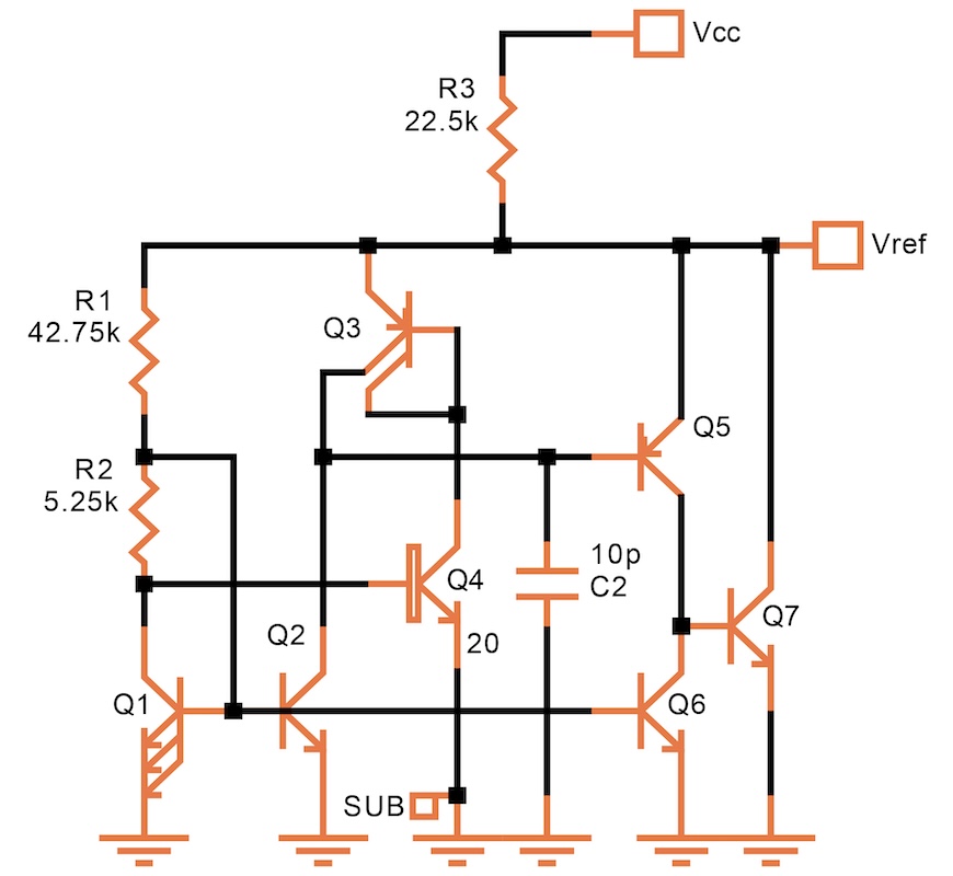
Figure 9-18. A similar bandgap circuit, but with a single VBE (1.25 V). [click to enlarge]
Here, the emitter ratio is 20:3. A second stage (Q5) increases the loop gain, lowering the output impedance to about 1.7 Ω. R3 is optimized for operation from 3 to 3.6 V, consuming 90 μA. Production variation from 0 to 100 °C is ± 2.2%.
Frequency compensation is a bit tricky. With a load capacitance of 500 pF or less, the circuit is stable and has a power supply rejection of:
- –80 dB below 10 kHz.
- –60 dB at 100 kHz.
- –40 dB at 1 MHz.
The circuit’s power supply rejection peaks at –40 dB.
A Bandgap Circuit with Increased Output Current Drive
Figure 9-19 shows the same circuit transformed into a three-terminal bandgap reference (a mini voltage regulator). It uses an NPN transistor, Q7, to supply the output current, which delivers a greater current than a (lateral) PNP transistor and makes frequency compensation an easy job. However, it only works down to a 2.2 V supply voltage.
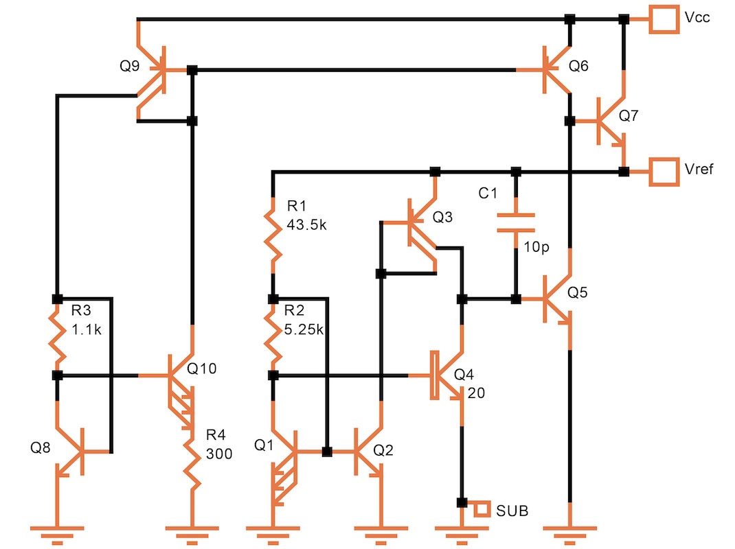
Figure 9-19. Three-terminal version of the circuit of Figure 9-18. [click to enlarge]
The base current for the output transistor is supplied by an independent current source consisting of Q6, Q8, Q9, and Q10. This is the self-starting current source we discussed earlier in the textbook.
Q5, the last transistor of the bandgap reference, diverts the unneeded current from Q6. Q6 supplies about 100 μA. At high currents, the maximum hFE of Q7 is about 100. Therefore, the output current is limited to about 10 mA to prevent burnout. Of course, the maximum output current also depends on the size of Q7.
Production variation (3σ) over a temperature range of 0 to 100 °C is ±2.4%. The output impedance is 1.5 Ω. The circuit is stable with any load capacitance.