Facebook
 Google
 GitHub
 Linkedin
The Brokaw Cell
Four years after Widlar developed his bandgap voltage reference circuit, Paul Brokaw published a paper entitled A Simple Three-Terminal IC Bandgap Reference. His actual circuit contained 14 transistors—not so simple after all. Figure 9-4 shows a version of the “Brokaw Cell” that includes only seven transistors.

Figure 9-4. The Brokaw cell with startup circuit.
The core of the Brokaw cell is formed by Q1, Q2, Q3, Q4, R1 and R2. The key characteristics of this circuit are:
- Q2 has 10 times as many emitters as Q1, so there is a ΔVBE of 60 mV across R1 at room temperature. The 10x ratio is an arbitrary choice—more would be better.
- Q3 is a current mirror, forcing Q1 and Q2 to run at the same current.
- Q4 completes the feedback loop from the collector of Q1 back to the input bias of the differential pair Q1/Q2 and supplies a moderate amount of output current.
When the circuit is in balance, a multiplied ΔVBE shows up across R2. Vref is, therefore, the voltage across R2 plus the VBE of Q1. The value of R2 is selected to achieve a zero temperature coefficient for Vref.
The gain in the feedback loop is limited, which eliminates the need for extra frequency compensation capacitors but results in a relatively high output impedance (about 80 Ω). Because of the emitter-follower output transistor (Q4), the minimum supply voltage is 2.2 V from 0 to 100 °C, or about 1 V above Vref.
The Brokaw cell needs a start-up circuit, which has been included in the left side of Figure 9.4. The chain of R3 in series with Q5 and Q6 always conducts. The voltage at the base of Q7 is, therefore, 2VBE. This ensures that Q7 pulls Vref up to one VBE, which is sufficient for Q1 and Q2 to start drawing current
Designing a Brokaw Cell for Low Supply Voltages
Figure 9-5 shows a modification of the Brokaw cell for operation at low supply voltage.

Figure 9-5. Three-terminal Brokaw reference with start-up for low voltage operation. [click to enlarge]
Output current is now supplied by Q6, which is a somewhat larger-than-normal lateral PNP transistor capable of delivering 5 mA. Q4 forms an additional gain stage, lowering the output impedance to 9 Ω.
Note that the operating current for Q4 is carefully set by Q5 and R3, with R3 having the same value as R2. In this way, the base currents of Q3 and Q4 cancel. Additionally, it means that Q1 and Q2 have identical collector voltages. The minimum supply voltage is now 1.6 V.
Choosing the Emitter Ratio
The design procedure for such a bandgap reference is very simple. First, you set the Q2/Q1 emitter ratio. For best matching, the two devices should use identical layouts for the emitters. Q2 just has more emitters.
Make the ratio as high as you can—with a ratio of 2:1, you get a ΔVBE of only about 18 mV, which puts a strain on the matching. At 10:1, the ΔVBE is about 60 mV (again at room temperature), and the matching requirements are less severe. At 50:1, the ΔVBE amounts to about 100 mV, at which point matching becomes easy. You also have a large number of emitters, which, statistically, improves matching.
With the emitter ratio chosen, you now know the value of ΔVBE appearing across R1. You then set R2 so that it drops about 600 mV. In this particular case, twice the current flows through R2 as flows through R1, so a 5:1 resistor ratio will give you a 10:1 voltage ratio.
Simulating the Brokaw Cell Bandgap Reference Circuit
Next comes the simulation. You’ll need good models—the resistor models must include the temperature coefficient. When plotting Vref against temperature, you’ll almost certainly see a marked temperature coefficient. Now simply change the value of R2 until this temperature coefficient is zero across the temperature range. A higher value for R2 will give you a more positive temperature coefficient.
Ideally, the ratio between R1 and R2 should allow you to divide them into identical sections in the layout. In this example, a 3 kΩ : 15 kΩ ratio would be perfect, breaking the divider into six identical sections of 3 kΩ each. In reality, this rarely happens.
You may find that you can get to this ideal ratio by changing the value of R1, thus drawing more or less current. If you can't, though, you can compromise by using a smaller basic resistor element (750 Ω, say). You can then create the odd value of R2 by making the last section (or perhaps the last few sections) a combination of parallel and series connections of that basic resistor element.
Figure 9-6 provides an example simulation of a bandgap voltage reference across temperature. Vref shows the characteristic bow of a bandgap reference due to the slight curvature of VBE. This amounts to about 0.18%.
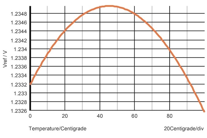
Figure 9-6. Characteristic bow in the temperature curve of a bandgap reference.
This curve was obtained using models for a simple 5 V bipolar process. The results are going to be different for other processes, so you’ll need to find the optimum value for R2 using your own models. The final value for Vref will most likely be somewhat different as well.
Dealing with Practical Limitations
When you plot Vref vs. temperature from a simulation, you get a false sense of precision. You will see the curve of Figure 9-6 only once in a while on a real IC, one that happens to have the exact nominal parameters.
Bandgap Reference Voltage Variation
What you have to live with is more like Figure 9-7, obtained from a Monte Carlo run.
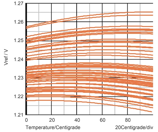
Figure 9-7. Monte Carlo analysis reveals the larger bandgap voltage variation that you will see in production.
Figure 9-7 shows a variation of about ± 2.5% over a range of 0 to 100 °C. This can be reduced by trimming. The best component to trim is R2. As you can see, there’s a distinct relationship between voltage and temperature coefficient, and R2 controls both.
Even with trimming, there’s a limit to accuracy. When a chip is attached to a lead-frame in a package, there is always some stress. The stress changes the bandgap potential. Unless some unusual precautions are taken, Vref can change as much as 0.5% (in either direction) compared to the value measured (or trimmed to) on the wafer. This can be avoided if the reference supports trimming in the package, of course.
Bandgap Reference Frequency Stability
The use of a PNP transistor at the output makes frequency compensation of a feedback loop difficult. This is especially true for a slow lateral PNP transistor.
About the only practical way to compensate this circuit is to place a large (external) at the output. Even so, a small resistor in series with the capacitor is required to create a zero (see the previous discussion of Frequency Compensation of Amplifier Circuits).
As illustrated by the transient pulse response in Figure 9-8, the loop is stable.
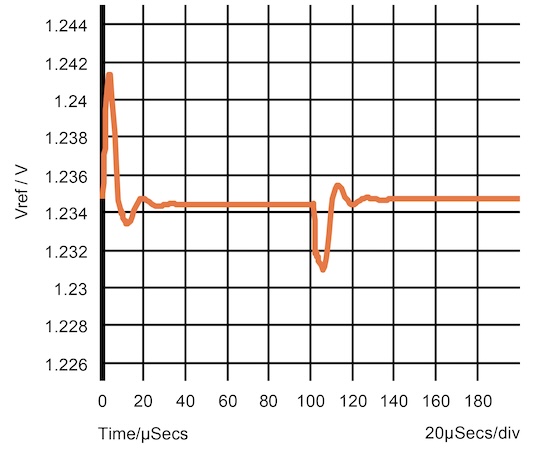
Figure 9-8. Pulse response of a Brokaw cell bandgap reference, indicating stability.
Power Supply Rejection
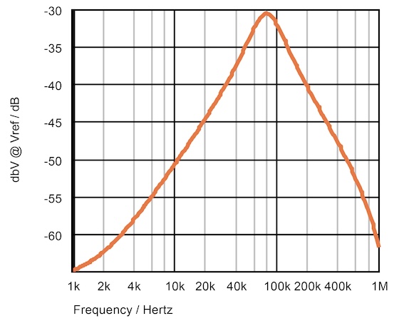
Another key consideration is the stability of the bandgap reference voltage —as illustrated in Figure 9-9, the power supply rejection of the Brokaw cell design at 100 kHz is a mere –30 dB.