Facebook
 Google
 GitHub
 Linkedin
Bandgap References
In February of 1964, David Hilbiber of Fairchild Semiconductor presented a paper at the Solid State Circuits conference titled "A New Semiconductor Voltage Standard.” Zener diodes were still very poor and he was looking for something that drifted less over time.
It was already known that transistors with base and collector connected together made almost ideal diodes. Hilbiber took two of Fairchild's discrete transistors with greatly different forward voltages (which he attributed to different diffusion profiles) and made two strings with different numbers of transistors (Figure 9-1).
Figure 9-1. Hilbiber’s 1964 voltage reference. [click to enlarge]
He found a current level at which, over the narrow temperature range of ± 2.5 °C, the voltage difference between the two strings changed little and amounted to 1.2567 V. He attempted to find a relationship between this voltage and the bandgap potential of silicon at zero Kelvin, but found that it was primarily a function of the semiconductor material used in the two different transistors. He got what he was after—a much better long-term stability—and stopped at that.
Widlar’s Bandgap Voltage Reference
Nothing happened for six years. Then, Bob Widlar put together the missing pieces. He recognized that the difference in diffusion profiles was only a secondary effect and that the idea would work better if the two transistors were made by identical processes.
If you plot the diode voltage (VBE) over temperature, as shown in Figure 9-2, you’ll notice that it points at the bandgap potential at absolute zero. Strictly speaking, this isn’t a straight line—instead, it’s slightly convex below about 150 °C and concave above it.
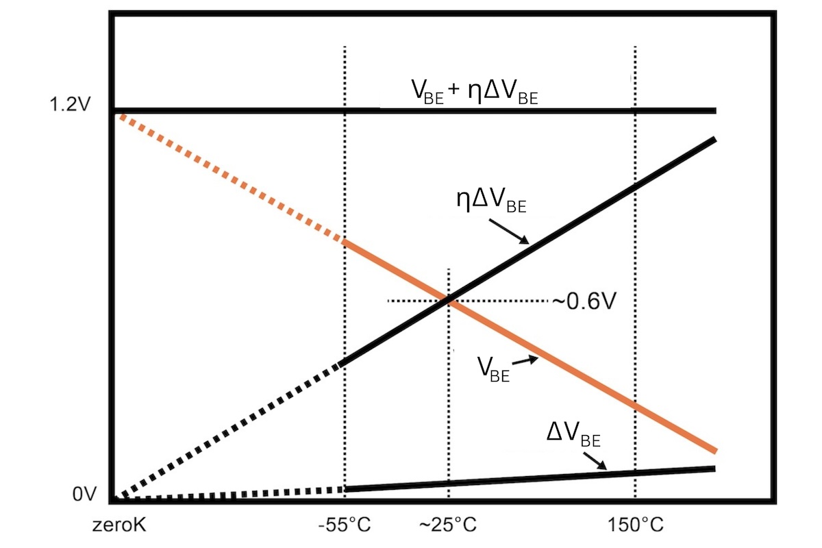
Figure 9-2. The principle of a bandgap voltage reference. [click to enlarge]
The bandgap voltage at zero K, by the way, is strictly a theoretical concept. At that temperature, there are no semiconductors. In fact, electrons don't move at all.
Widlar found that an equal but opposite temperature coefficient can be created by running two transistors at different current densities:
$$\Delta V_{BE} ~=~ \frac {kT}{q} ~\times~ \text{ln} \bigg( \frac {A_1 I_2}{A_2 I_1} \bigg)$$
where A is the effective emitter area of each transistor, and I is the current running through it. Here you have the choice of either using different emitter sizes, different current levels, or both at the same time.
ΔVBE is a true straight line, pointing to zero at zero K (as illustrated above in Figure 9-2). However, it’s relatively small. kT/q amounts to about 26 mV at room temperature, so an area (or current) ratio of 10 gives you a ΔVBE of about 60 mV.
As you can see from the plot in Figure 9-2, you need about 600 mV at room temperature to counteract VBE. But Widlar came up with a simple solution: multiply ΔVBE with a resistor ratio. The resulting circuit is shown in Figure 9-3.
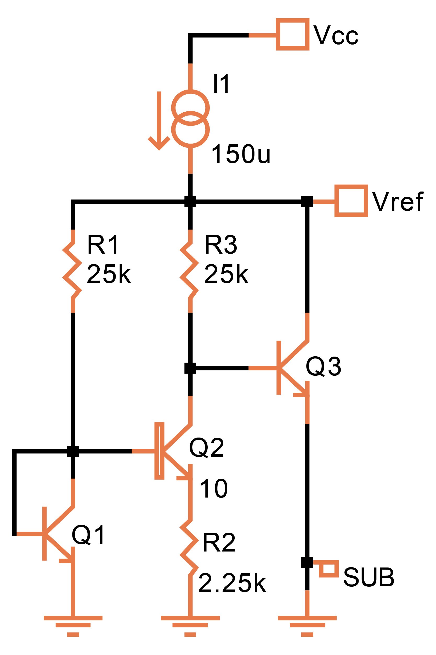
Figure 9-3. Widlar's bandgap reference. [click to enlarge]
In the circuit above, R1 creates a current in Q1. Q2 has ten times the emitter area of Q1, so there is a ΔVBE between the two transistors of about 60 mV at room temperature. This ΔVBE shows up across R2.
Ignoring a small error due to the base current, the emitter and collector currents of Q2 are equal. Thus, the voltage drop across R3 is ΔVBE multiplied by η, the ratio of R3 to R2.
By adding the VBE of Q3 to this voltage, we get Vref. The three transistors form a feedback loop that holds Vref at a constant level. The gain of this feedback loop is limited, which is why the internal capacitances are sufficient to keep it from oscillating.
If we increase the value of R3, Vref increases, and the positive temperature coefficient increases. If we decrease R3, the opposite happens. In this way, we can find the right value for R3 so that the negative temperature coefficient of VBE is canceled by the positive temperature coefficient of ΔVBE.
Widlar's first design was a bit more complicated than the one shown in Figure 9-3. It used 14 transistors and produced 5 V with four diode-connected transistors in series. The ΔVBE multiplication factor was about 40. It is no longer used.
Limitations of the Bandgap Voltage Reference
There’s no such thing as an absolutely precise bandgap voltage. Instead, you’ll find that the voltage at which Vref has no temperature coefficient can be anywhere between about 1.18 V and 1.25 V. This is due to several effects, namely:
- The bandgap voltage is slightly dependent on the doping level.
- The bandgap potential of a semiconductor changes with pressure (or stress).
- We’re presumably using diffused resistors, which have temperature coefficients of their own.
- As pointed out before, VBE vs. temperature isn’t an exact straight line, so Vref vs. temperature will always show a slight upward bow.
Nevertheless, such a bandgap reference voltage can have an accuracy of better than ± 3% without trimming any of the components.
Apart from base currents, which can be compensated for in more advanced designs, there are two main sources of error in a bandgap reference:
- VBE. This is an absolute value, not a ratio. You have to rely on the precision with which dopants can be introduced into silicon during the process. In a well-controlled process, this amounts to about ± 10 mV uncertainty, or about 0.8%. Be aware that prototypes from a single wafer (or even a single run) will not give you any indication of how much this varies in production over many wafers.
- Ratios. In Widlar's first bandgap reference there are three ratios of significance: Q1/Q2, R3/R2, and R1/R3. To minimize these errors, you simply make these devices large.