Facebook
 Google
 GitHub
 Linkedin
Improved CMOS Current Mirrors
Unlike bipolar current mirrors, the base current problem does not exist with CMOS devices, they require no input current. As shown in Figure 4-19, you are free to add as many dependent current sinks as you desire if the change in current with output voltage doesn't bother you.

Figure 4-19. Multiple parallel current mirrors in MOS.
If this voltage dependence is too large, you have the choice of increasing the gate lengths, adding resistors in all sources, or—you guessed it—adding a few devices.
Cascode MOS Current Mirror
To reduce the influence of the output voltage, we could use the Wilson current mirror, as discussed in our section on Improved Bipolar Current Mirrors. But MOS devices cannot take advantage of one of its features, the cancellation of base currents.
For this reason the Wilson current mirror is not the best choice for MOS, a simple cascode stage has slightly better performance and can be made to have a wider range in the output voltage (Figure 4-20).
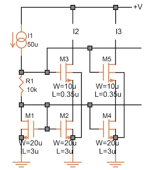
Figure 4-20. Current mirrors with cascode transistors.
Here M3 and M5 simply shield M2 and M4 from changes in the output voltage. Their gates are held at a voltage slightly higher than the threshold voltage of M1 by causing a voltage drop in R1.
In our case here, this bias voltage is 500 mV, which results in quite a remarkable performance, as illustrated in Figure 4-21, but requires at least 0.7 V at the output. Lowering the voltage drop across R1 lowers this minimum output voltage but increases the voltage dependence, which you can reduce again using even larger devices.
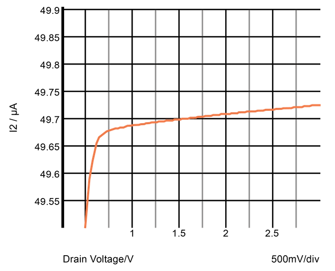
Figure 4-21. Performance of cascode MOS current mirror.
Again, don't get carried away by the impressive performance shown with the single sweep shown in Figure 4-21, which assumes perfect matching. A Monte Carlo run will show you the true behavior (Figure 4-22).
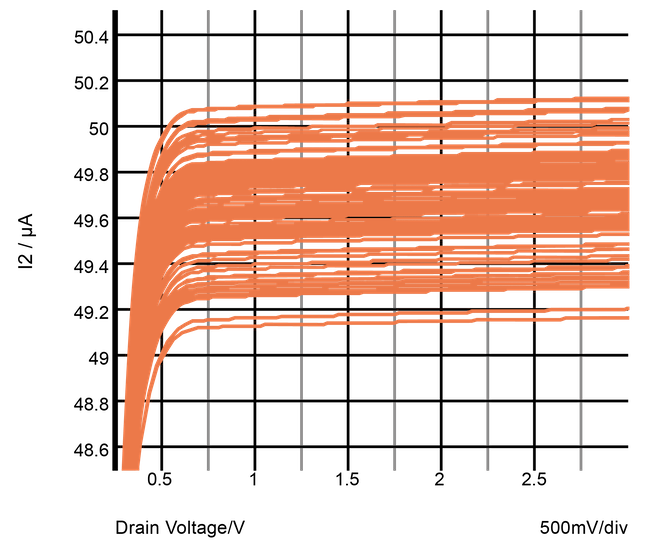
Figure 4-22. Monte Carlo simulation of the cascode MOS current mirror.
Additional Design Techniques for CMOS Current Mirrors
For CMOS current mirrors, there are three more sophisticated schemes. Figure 4-23 is the one you frequently see in articles.
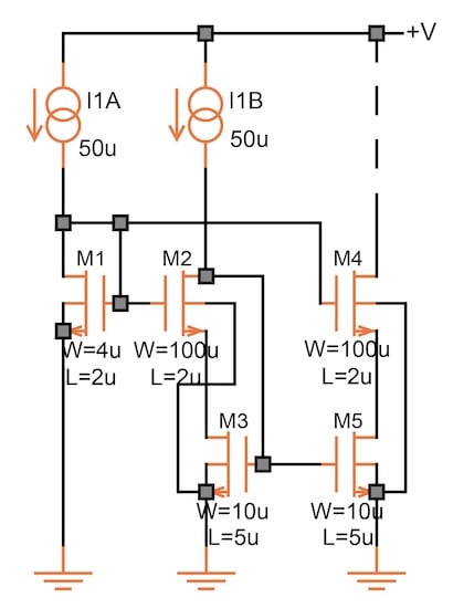
Figure 4-23. Widely used MOS current mirror.
M1 is a thin device, producing a bias voltage about 100 to 200 mV higher than the gate voltages of M3 and M5. Since the gates of M2 and M4 are connected to this point, these two devices act as cascodes, i.e., they shield the lower two devices from voltage changes.
Alternatively, the circuit in Figure 4-24 using the dimensions shown has exactly the same performance with fewer devices and less current consumption. Here the lower devices are dimensioned so that the gate voltage (at 50 μA) has the required value for cascode biasing.
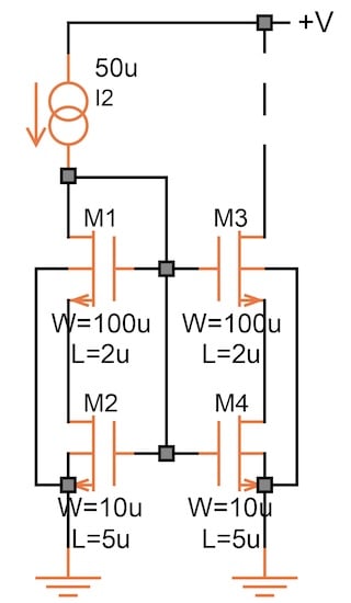
Figure 4-24. A MOS current mirror with fewer devices that provides the same performance.
The upper devices are then made wide enough to leave a comfortable margin between their source potentials and the "on" voltage of the lower devices (i.e., the voltage drop caused by channel resistance). This is a prime example of how much you can do by simply changing the channel length and width of a CMOS transistor.
The circuit in Figure 4-25 has the best performance. The cascode bias voltage is set not only by the device dimensions but by the small (250 mV) voltage drop across R1. Since the current itself is almost certainly determined by a resistor, R1 will track it.
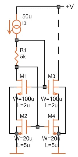
Figure 4-25. A MOS current mirror with the best performance.
The flatter curve shown in Figure 4-26 represents a higher output impedance (100 MΩ for the circuit of Figure 4-25, 33 MΩ for the circuits of Figures 4-23 and 4-24) which is important for high gain in active loads.
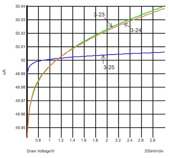
Figure 4-26. MOS current mirror performance comparison.
All the figures given here are for room temperature only. The threshold voltage, the resistor and, in bipolar designs, the VBE have temperature coefficients. Make sure you simulate your circuit over the entire temperature range.