Facebook
 Google
 GitHub
 Linkedin
The Simple Current Mirror
The Wild Widlar
Bob Widlar was a truly great designer of analog ICs. He was wild and totally unmanageable and had an odd sense of humor. The press loved him, and he had a flair for self-promotion. He shunned computer analysis, preferring to breadboard his circuits, but time and time again, he came up with nuggets of design details and products that were thought to be impossible. Burned out by the frenzy of Silicon Valley, he moved to Mexico, where he died in 1991 at age 53.
One of Widlar's early contributions was the current mirror, a design detail (or design element) that you will now find in just about any analog IC. Here, we’ll discuss the simplest bipolar and MOS versions of the current mirror.
The Simple Bipolar Current Mirror
To understand the current mirror in Figure 4-1, let's start by considering the primary current, I1, which flows into the diode-connected transistor Q1. This produces a voltage drop across the base-emitter diode of Q1. This voltage drop is called VBE.
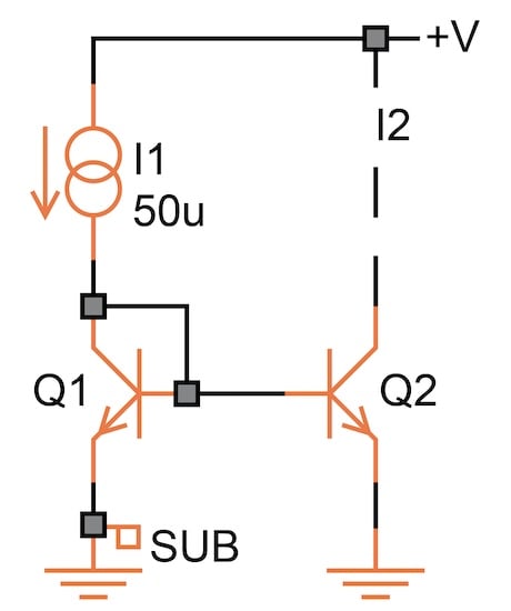
Figure 4-1. A simple bipolar current mirror.
Now connect the base and emitter of a second, identical transistor, Q2, to the same nodes as those of Q1. Since the base-emitter voltage of Q2 is the same as that of Q1, it follows that its collector current should be the same as that of Q1’s collector current, and so I2 = I1.
Non-Ideal Behavior of the Simple Bipolar Current Mirror
Well, not so fast. There are errors in this assumption—two of them. The first one concerns the base currents. I1 splits into three paths: the collector current of Q1 and the two base currents:
$$I_1 ~=~ I_{c1} ~+~ I_{b1} ~+~ I_{b2}$$
Therefore, the collector currents for Q1 and Q2 are both smaller than the primary current (I1):
$$I_{c2} ~=~ I_{c1} ~=~ I_1 ~-~ (I_{b1} ~+~ I_{b2})$$
Assuming a minimum current gain of 100, each base current amounts to 1% of the collector current, for a total of 2%. So the collector currents of Q1 and Q2 are 2% smaller than I1, worst-case.
The two transistors may be identical, but assuming that they’re operated identically is error number two. The collector voltage of Q1 is always VBE, but the collector voltage of Q2 may be anything. As we know from the discussion of the performance limitations of bipolar transistors in the Analog Devices chapter, the gain is affected by the collector voltage. Due to the Early effect, it increases as the collector voltage increases. Thus I2 isn’t exactly steady, as Figure 4-2 illustrates.
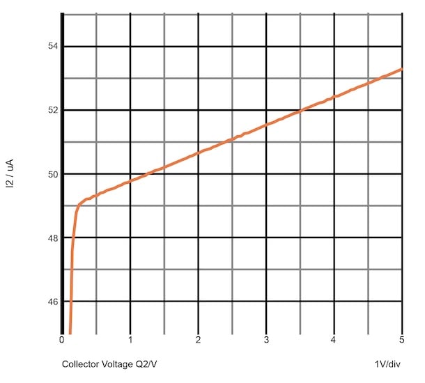
Figure 4-2. Current vs. collector voltage for a simple bipolar current mirror.
In Figure 4-2 (and all other simulation examples in this chapter), the current reference I1 is 50 μA. For this particular transistor, which is made in a process capable of 20 V, I2 changes by 8% over the range of the collector voltage. It increases from about 49 μA at 0.3 V, which is the saturation voltage of Q2, to about 53 μA at 5 V.
This is the simplest current mirror. As we’ll see later on in the chapter, we can improve its performance considerably with additional devices.
The Lateral PNP Current Mirror
There’s also a lateral PNP equivalent of the simple current mirror, which is shown in Figure 4-3.

Figure 4-3. Current mirror using a lateral PNP transistor.
Because it uses a split collector, this current mirror needs only a single device. Since each collector is smaller, the maximum current is more limited (depending on the process, about 100 μA). Figure 4-4 shows the voltage dependence of the PNP current mirror.

Figure 4-4. Voltage dependence of I2 for the lateral PNP current mirror.
The voltage dependence of a PNP current mirror is generally a bit worse than that of an NPN design (here, about a 12% change). The voltage of the second PNP collector can move to within about 0.3 V of the positive supply voltage (+V). If you let it go any higher, or disconnect the collector completely, you get a substrate current about equal to I1.
Special Note: The Current Source
All current mirrors start with a current source (I1 in Figure 4-1) from which one or more currents are derived. For ICs, a current mirror is a more basic element than a current source, which is why they’re discussed first in this textbook.
However, be aware that there’s a significant difference between a theoretical or simulated current source and a practical one. In a simulation, a current source will do anything to keep its programmed current level, including building up thousands of volts. In an actual circuit, the supply voltage limits the excursion.
Also, little distinction is usually made between a current source and a current sink (for example, I1 in Figure 4-3). For convenience, both of them are usually termed current sources.
The Simple MOS Current Mirror
The current mirror also works with MOS devices, as we see in Figure 4-5.

Figure 4-5. Simple MOS current mirror.
Figure 4-6 shows the voltage dependence of the MOS current mirror in Figure 4-5.
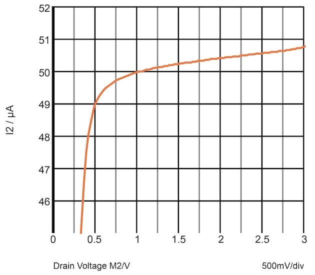
Figure 4-6. The voltage dependence of the simple MOS current mirror.
The voltage dependence can be reduced by increasing the channel lengths of the MOSFETs. Figure 4-6 shows only about a 1.5% change in current over the 1 V to 3 V range of the drain voltage for this 0.35 μm process. However, that’s because the channel lengths were made quite large.
It takes at least 0.5 V at the drain of M2 to make the mirror work, a figure which you can improve by making the devices much wider. The mirror can be inverted by using P-channel devices.