Facebook
 Google
 GitHub
 Linkedin
Improved Bipolar Current Mirrors
Let’s see how we can improve the performance of the basic current mirror.
Emitter Resistors
A first step is to connect resistors to the emitters (or the sources, in the case of MOS transistors), as illustrated in Figure 4-7.
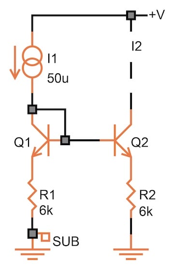
Figure 4-7. Improved current mirror with emitter resistors.
With the 6 kΩ resistances we’re using in this example, we drop 300 mV across the resistors. If the current in Q2 wants to be higher than I1, it would also cause a higher voltage drop across R2.
This increased voltage drop across R2 decreased the base-emitter voltage (VBE) of Q2. This negative feedback effect forces I2 back to where it’s more or less equal to I1. There is, however, still the base current error, which isn’t improved.
There is a penalty associated with using the emitter resistors: the voltage at the collector of Q2 can’t go any lower than the voltage drop across R2 plus the saturation voltage of Q2. In this case, that’s about 600 mV total. From 600 mV to the supply voltage (5 V), I2 only changes by about 0.7%, as we see in Figure 4-8.
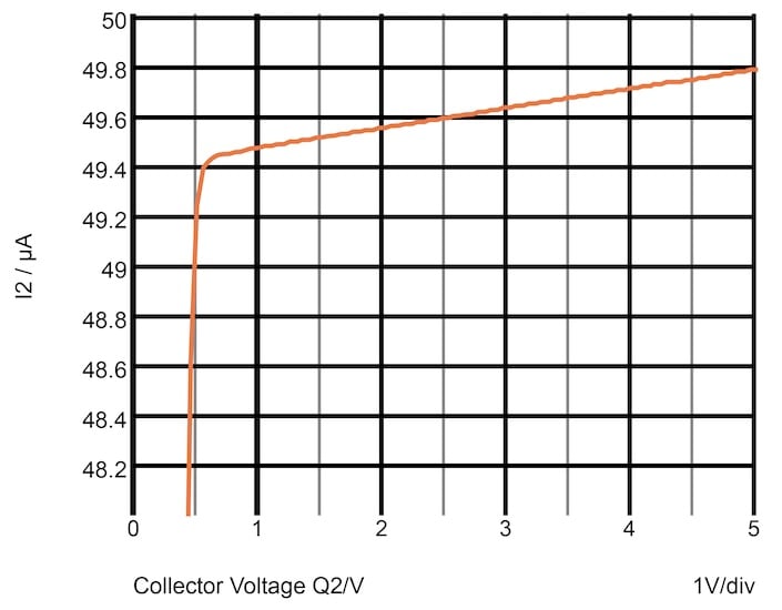
Figure 4-8. Emitter resistors reduce the current mirror voltage dependence to 0.7%.
A measure of the quality of a current source is its output impedance, which is the change in voltage divided by the change in current. The original current mirror had an output impedance of 1.1 MΩ. This has now increased to 12 MΩ.
As a final note, if you want to use emitter resistors in the PNP equivalent of the Widlar current mirror, you’ll need to use two separate transistors rather than a split collector.
The Widlar Current Mirror: A circuit similar to Figure 4-7 has become known as the Widlar current mirror. In the Widlar current mirror, the emitter resistor is only included with the output transistor (Q2).
The Wilson Current Mirror
An even greater improvement can be made with the addition of a transistor. This circuit, invented by George Wilson, is naturally called the Wilson Current Mirror (analog designers don't get Nobel prizes, they get a circuit named after them). Figure 4-9 shows a basic Wilson current mirror.

Figure 4-9. Wilson current mirror.
In the Wilson current mirror, Q3 acts as a cascode stage—its sole job is to shield the important matching transistors, Q1 and Q2, from any fluctuation in the output voltage. It does this job and more: by a happy coincidence, the three base currents cancel. Figure 4-10 shows the performance of the Wilson current mirror.
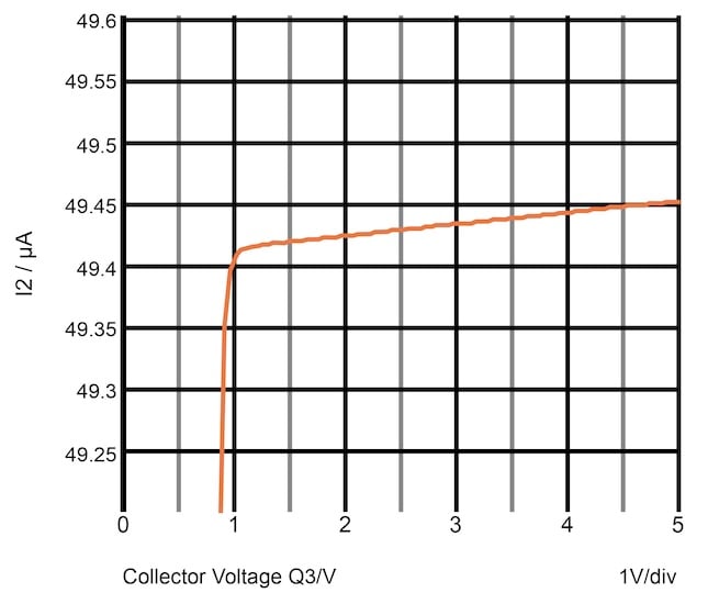
Figure 4-10. Performance of the Wilson current mirror.
In Figure 4-10, I2 is now within about 1% of I1 and changes only about 0.09% over the useful voltage range (an output impedance of 90 MΩ). Note, however, that the useful voltage range stops at a little over 1 V, given by the VBE of Q2 plus the saturation voltage of Q3.
The PNP Wilson Current Mirror
Naturally, there’s a PNP equivalent of the Wilson current mirror, as illustrated in Figure 4-11. This time, we can use a split-collector device for Q1.
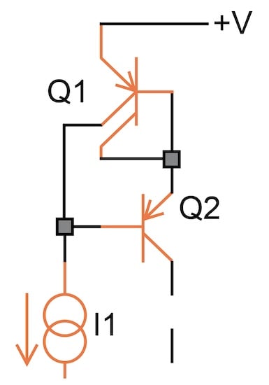
Figure 4-11. PNP version of the Wilson current mirror.
At room temperature, the output voltage can go to within about 1 V of the supply voltage (+V). Here, the improvement isn’t quite as good as the NPN version of the Wilson current mirror—the output current changes by about 0.5%.
Removing an Error in the Wilson Current Mirror
There’s still a systematic error in the basic Wilson current mirror: the two transistors intended to match don't have the same collector voltages. One transistor is at VBE; the other is at 2VBE.
In the relentless pursuit of perfection—a trait given at birth to all analog designers—we shall now proceed to eliminate it. Enter a fourth transistor (Figure 4-12).
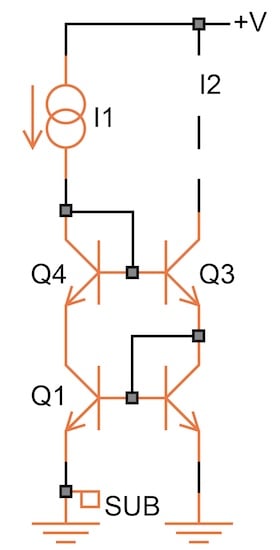
Figure 4-12. Four-transistor mirror.
The only purpose of Q4 is to lower the collector voltage of Q1 to the same level as that of Q2. With this, we see in Figure 4-13 that I2 is now within 0.6% of I1 and changes by less than 0.08% over the output voltage range.
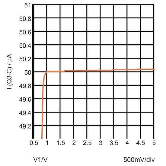
Figure 4-13. Performance of the four-transistor current mirror.
The single sweep in this DC analysis is, however, deceiving. The depicted curve can only be observed once in a great while—when all four devices match perfectly. Only a Monte Carlo analysis can tell you what will really happen in production. Figure 4-14 provides one.

Figure 4-14. Monte Carlo analysis of the 4-transistor bipolar current mirror.
As the Monte Carlo analysis shows, we definitely have a remarkably small change with output voltage, but the output current will vary by ± 3% because of mismatch.