Facebook
 Google
 GitHub
 Linkedin
Layout of CMOS Transistors
When using the basic layers only, the layout of an N-channel transistor is quite simple. There are only three patterns, the first of which is the poly gate (which sits on top of a thin oxide).
The second pattern delineates an N+ implant. It is simply a rectangle, protruding from either side of the poly gate. The N-type dopants enter the P-type silicon substrate only outside the gate area. The implant is blocked by the polysilicon gate.
The third mask places contact openings in the poly and implanted regions.
For a P-channel device, two additional masks are required:
- One for an N-well.
- One for the P+ implant.
The N-well must surround the device or devices. Additionally, it must be contacted and biased.
The patterns in Figure 19-12 show long channels, which are often required in analog design. In the figure, the channel length is from left to right, and the channel width is from top to bottom.
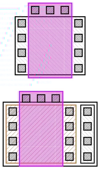
Figure 19-12. Layout of N-channel (top) and P-channel (bottom) transistors.
Practical CMOS Layouts
Alas, if only things were that simple. In reality, the layout of CMOS ICs always involves a large number of masks. Layers include:
- Field implant.
- Threshold implant.
- Poly 2.
- Poly 3.
- Metal 2.
- Metal 3.
- Metal 4 (and so on).
- Interconnections between the metal layers (vias).
- Pad mask.
Furthermore, additional layers use masks created from combining other patterns. These layers are not drawn directly. Instead, they are coded.
Most CMOS processes have an N-well for the P-channel devices. The N-channel devices typically sit in the common substrate. Sometimes, both N-wells and P-wells are present.
Drain and source are interchangeable. This enables a peculiar but efficient way to connect devices in parallel to increase the channel width. As shown in Figure 19-13, you connect them in series and merge the terminals between the gates. The source of one transistor also acts as the drain of the next one, saving space.
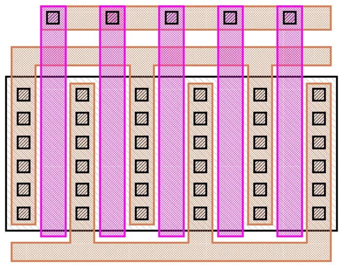
Figure 19-13. Parallel connection of N-channel transistors.
The smallest possible set of matching devices consists of four transistors arranged to be point-symmetrical. This arrangement is illustrated in Figure 19-14.
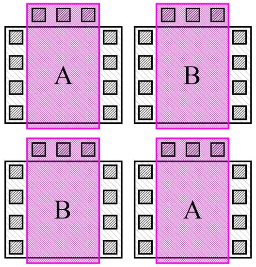
Figure 19-14. A matching pair of N-channel transistors, using four devices.
In the above figure, the connections between the transistors are not shown. To create the matched pair, the terminals of the two transistors labeled A must be connected together. Similarly, the terminals of the two B transistors must be connected. You will find that this is almost impossible without employing the second metal layer.
If there is a gradient (thermal or otherwise), it will affect both devices equally, no matter which direction it takes.