Facebook
 Google
 GitHub
 Linkedin
Layout of Resistors in IC Processes
In a diffused resistor, there is always a surrounding semiconductor region. This is shown in Figure 19-10. For a bipolar process, this is the epitaxial layer. In CMOS, it's a well or the substrate.
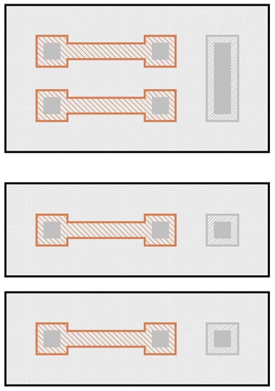
Figure 19-10. Diffused resistor pairs in a common island (top) and in separate islands (bottom).
This surrounding region needs to be at a voltage potential such that the junction is reverse-biased. The bias voltage causes a depletion layer to extend into the resistor, decreasing its cross-section and thus increasing its resistance. For a base diffusion, this effect is small (about 1%) but not always negligible. For an implanted resistor, it can be very large (20%).
Thus, if two diffused resistors form a voltage divider, the difference between the bias voltage and the resistor voltage is larger for the lower resistor than the upper one, resulting in a shift of the divider ratio. It may be small enough to ignore for resistors with 200 Ω/□ (about 0.2%), but for implanted resistors, this error is almost always significant. Note that this is an initial error only; it is not subject to change during production.
To avoid this effect, you can place each resistor in its own tub and connect the tub to the positive end of the resistor.
Minimizing the Seebeck Effect
Routing the metal also needs some thought. The Seebeck coefficient causes the metal contacts at the ends of the resistors to produce a voltage if the ends are at different temperatures. Therefore, it's advantageous to keep connections close together so that a thermal gradient will have the smallest effect.
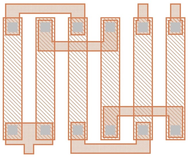
Figure 19-11 shows a pair of resistors with three sections each. In the lower left, these two resistors share a common connection. In the upper right, the two resistor contacts are close together to obtain the shortest distance. For optimum matching in the presence of a thermal gradient, the sections also alternate.