Facebook
 Google
 GitHub
 Linkedin
Layout of Bipolar Transistors
The layout of analog ICs has so far remained an art. There are no computer programs that can design, place, and route the components in an intelligent, competent way. More often than not, the person who created the circuit diagram needs to get involved.
This chapter is by no means a complete guide—it would take an entire book to do the subject justice. Look at it as some hints stemming from practical experience.
Masks for a Bipolar Process
The minimum sequence of masks in a bipolar process is:
- Buried Layer.
- Isolation.
- Sinker.
- Base.
- Emitter (N+).
- Contact.
- Pad.
The last mask opens up windows over the bonding pads in a thick glass layer.
Note that the emitter mask is also used to make a low-resistance contact to the collector (the epitaxial layer).
To these seven basic masks, several others may be added:
- A second (often identical) isolation mask, applied after the buried layer (but before epitaxial growth), to implant P-type regions which diffuse upward (up-down isolation).
- A separate mask for high-value (implanted) resistors.
- A mask for Schottky diodes, which can consist either of aluminum or barrier metals directly in contact with the epi layer.
- An additional mask for P+ regions, sometimes used to improve the performance of lateral PNP transistors.
- A mask for thin-film resistors.
Occasionally, a washed emitter is used. Here the emitter diffusion (or more likely, implant) takes place through the N+ contact openings (while the windows to the P-regions are masked off). After creating the N+ regions, the thin oxide layer over them is simply etched (or washed) off without a mask. In this way the emitter area can be made smaller, because it is self-aligned with the contact window.
The dimensions of the mask patterns are determined by the process. Some of the factors are:
- Minimum size of contacts: Determined by how small a window can be etched into the oxide. Most of the small-geometry processes require all contacts to be of identical size.
- Distance between emitter and base contacts: Usually given by the minimum required spacing of the metal covering them.
- Overlap of metal over contacts: Determined by how well the metal can be aligned to the contact.
- Spacing between sinker and base: Set by the sideways diffusion of the sinker (and base) and the depletion layer width for the maximum voltage.
- Spacing between base and isolation: Determined by the sideways diffusion of the isolation (and base) and two depletion regions.
- Spacing between sinker and isolation: Must accommodate two sideways diffusions and one depletion region.
- Spacing between buried layer and isolation: Must allow for the sideways diffusion of both the isolation and the buried layer.
- Difficulty aligning to the buried layer: After epitaxial growth, the image of the buried layer at the surface is blurred and shifted along the crystal axis. This results in the least accurate alignment.
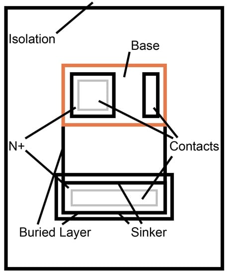
Figure 19-1. Mask layers for an NPN transistor.
The isolation mask is a special case. The diffusion takes place between the devices, but it would be awkward to draw such a complex web. Thus, a convention has been established to draw the isolation region where it is not, and then invert the pattern on the mask.

Figure 19-2. Isolation pattern.
NPN Transistor Designs
There are several choices for the design of an NPN transistor. Figure 19-3 shows some of them. For clarity, the buried layer and sinker patterns have been omitted.
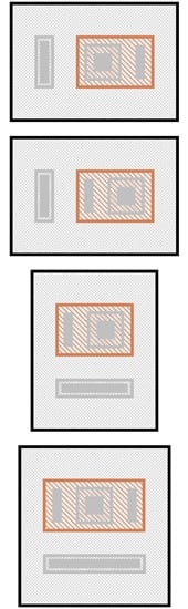
Figure 19-3. Small NPN transistor patterns.
In the top pattern the emitter is in the center, the base contact on the right, and the collector contact on the left. In the pattern directly below it, the emitter and base contact are reversed. There is a slight advantage to having the emitter closer to the collector contact, in that the distance the current has to travel in the buried layer to a point underneath the emitter is reduced.
You will also see NPN transistor patterns with more space between emitter and base or base and collector to accommodate metal lines.
In the third pattern, the collector contact has been moved. This results in a somewhat lower saturation voltage.
The bottom pattern contains two base contacts, effectively doubling the current capability of the devices. To understand this, remember that the maximum current is given by the effective emitter length, i.e., the length of the emitter facing the base contact. The rest of the emitter area is ineffective at high currents.
Two-Emitter NPN Transistors
Figure 19-4 shows NPN transistors with two emitters in a single island (or tub).
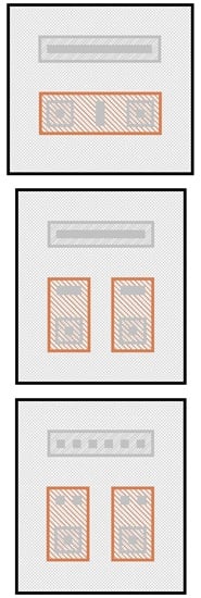
Figure 19-4. Two-emitter NPN transistors.
In the top pattern collector and base are common, meaning that they are connected together. This limits the usefulness of the device.
In the center pattern there are separate bases—only the collector is common. The bottom pattern is identical, with the contacts redrawn for uniform size.
There is a danger to having multiple emitters in the same island. As mentioned before, the image of the buried layer is shifted (at least, in all but low-pressure epitaxial processes). The actual buried layer region is a rectangle covering the area from the collector contact (and sinker) to the far edges of the base regions. But the image appearing on the surface is shifted along the crystal axis.
Epi-Shift
In silicon starting material, with the wafer flat at the bottom, the epi-shift is to the right. This is illustrated in Figure 19-5.
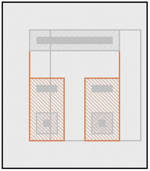
Figure 19-5. Epi-shift influencing one emitter but not the other.
The amount of shift is roughly equal to the thickness of the epi-layer. What we see on the surface is a depression, caused by a slight consumption of silicon during the diffusion of the buried layer. It is therefore likely that this step in surface height will hit the left emitter, but not the right one, which influences their matching.
This effect can be avoided if the entire transistor is rotated so that the edge of the shifted pattern falls between the collector contact and the bases. Figure 19-6 shows this with a two-transistor layout. The center transistor has a single emitter, while the outer one has 16. This layout is used, for example, in a bandgap reference.
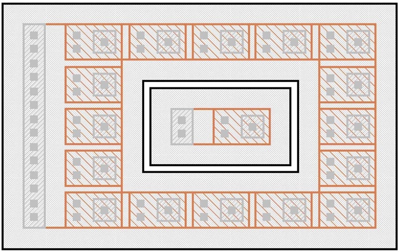
Figure 19-6. 16:1 emitter ratio with epi-shift mismatch avoided.
Higher-Current NPN Transistors
The transistor patterns shown so far are all intended to be the smallest possible size, which naturally limits how much current they can carry. To increase the current capability, the effective emitter length needs to be increased. For the NPN transistor in Figure 19-7, not only have the emitters been tripled and stretched, but base contacts have been placed on both long sides.
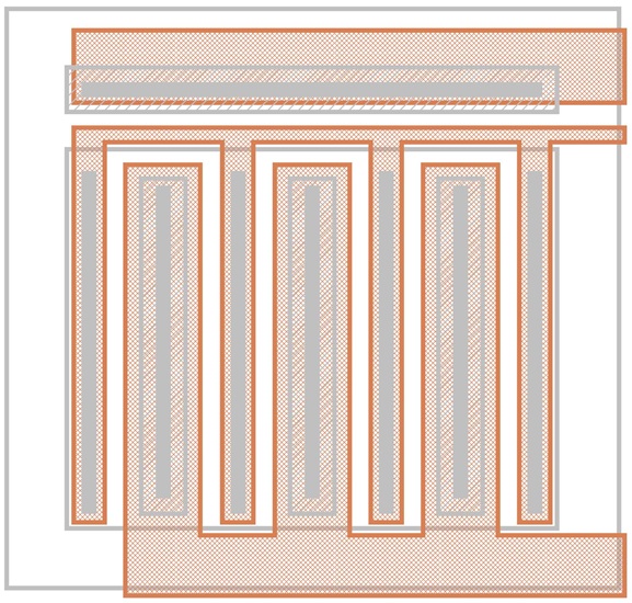
Figure 19-7. NPN transistor for higher current.
Note that the increase in current capability almost always requires wider metal runs for both the emitter and collector.
An alternate design is shown in Figure 19-8, with the uniform contact openings required by dense processes. There are two collector contacts on the outside, three emitters, and four base contact columns.
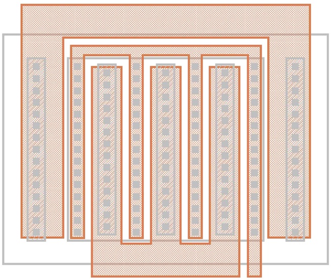
Figure 19-8. Alternate high-current design.
If you increase the size of such a transistor further, there comes a point where it's advantageous to taper both the emitter and collector metal, gradually increasing the width as the currents from more and more contacts are added.