Facebook
 Google
 GitHub
 Linkedin
Low-Dropout Regulators
To get a lower minimum voltage drop, we need to replace the NPN Darlington transistor at the output of Figure 16-1 with a PNP (or P-channel) device. The result is shown in Figure 16-7.
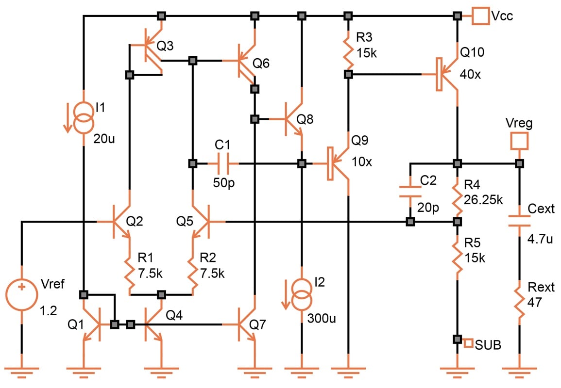
Figure 16-7. [click to enlarge] Low-dropout regulator with internal (lateral) PNP transistor at the output.
And here is where the problem starts. Output transistors need to be large to carry the current. They therefore have substantial capacitance, which is multiplied by the Miller effect. This forms an additional pole, which gives the regulator a stubborn tendency to oscillate.
It takes three capacitors to quiet down this regulator:
- C1 provides the main pole at about 30 Hz.
- C2 corrects the phase at very high frequencies.
- Cext, together with Rext, forms a zero at 1 kHz.
In addition, the loop gain is reduced with R1 and R2. Even so, Figure 16-8 shows that the phase margin is barely 50 degrees.
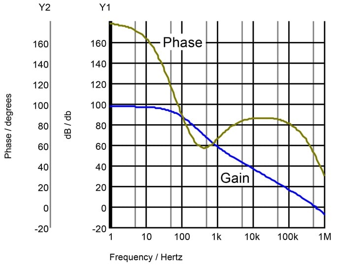
Figure 16-8. Phase/gain diagram using three compensation capacitors.
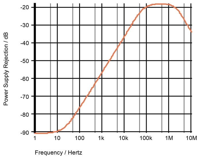
The power supply rejection versus frequency is shown in Figure 16-9.
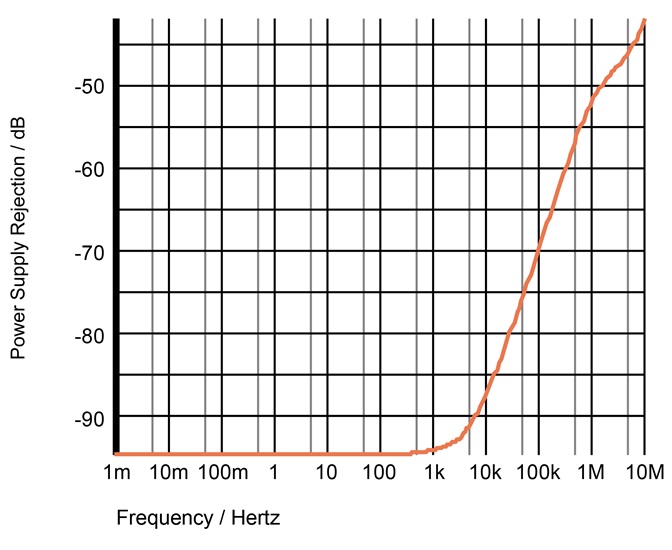
Figure 16-9. Power supply rejection.
The external capacitor offers the benefit of increased power supply rejection, but its effectiveness is limited by the series resistor (which is essential to form the zero and turn the phase back up). The power supply rejection versus frequency is shown in Figure 16-9. At frequencies above about 5 kHz, the power supply noise appearing at the output is simply determined by the collector capacitance of Q10 and Rext.
Q10 is a large lateral PNP transistor with an effective emitter length 40 times that of a small device, which makes it capable of carrying about 20 mA. The dropout voltage at this current is shown in Figure 16-10.
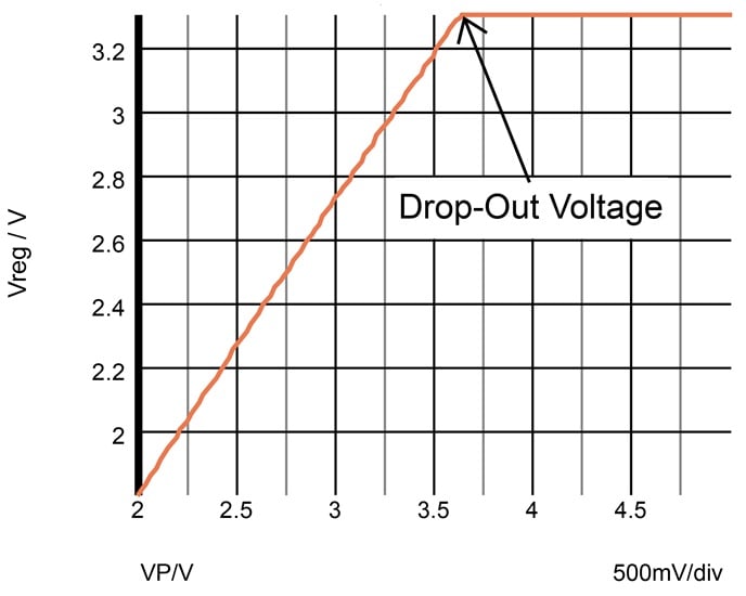
Figure 16-10. Dropout voltage at 20 mA.
As we see above, the dropout voltage at 20 mA is 300 mV. The output impedance is 4 mΩ.
Current capability can be increased at will, simply by making the output transistor larger. Low-dropout regulators using lateral PNP transistors have been built for up to 5 A. Specialized semiconductor processes provide a higher doping level for the emitter, improving performance at such high current levels. Even so, the output devices take up some 80% of the chip area. Be aware that, as the lateral PNP transistor saturates at the dropout voltage, its substrate current becomes very large.
High Currents in an IC
There are two factors that limit how much current an IC can carry. The first is electromigration. The force of huge numbers of electrons rushing through a conductor can become so large that the electrons begin to move atoms, physically pushing them along. Electromigration is aggravated by high temperature and depends on the composition and grain structure of the metal.
For pure aluminum, this happens at about 500,000 A/cm2. The effect is slow—it may take months. Eventually, though, there will be an area where there is no aluminum left.
Half a million amperes may seem large and safe, but when you consider that you are dealing with very thin layers, the limitation becomes real. For example, for a thickness of 10,000 Angstroms (10,000 Å = 1 μm) and a width of 1 μm, a current density of 500,000 A/cm2 is reached with just 5 mA.
The second limitation is resistance. Pure aluminum has a resistivity of 2.8 μΩ·cm. Thus, a layer that is 1 μm thick has a sheet resistance of 28 mΩ/◻. Make this run 100 μm long and you have a resistance of 2.8 Ω.
Let's say you want to carry 1 A over a distance of 1,000 μm on a chip. With a thickness of 1 μm, the aluminum stripe would have to be at least 200 μm wide to avoid electromigration. It then would have a resistance of 140 mΩ, giving it a voltage drop of 0.14 V.
And don't forget to check how much current contacts and vias can take in your process, as well as the thickness required for bonding wires.
Low-Dropout CMOS Regulator
Figure 16-11 shows a CMOS version of Figure 16-7.
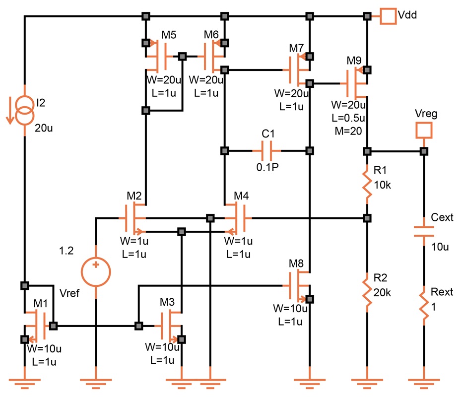
Figure 16-11. [click to enlarge] Low-dropout CMOS regulator.
Also dimensioned for 20 mA, the P-channel output device is smaller than the previous lateral PNP transistor. A low dropout voltage is, however, only present at low current. To get the same value at 20 mA, M9 would need to be 20 times the indicated size, for a total width of 8,000 μm. This is illustrated in Figure 16-12.
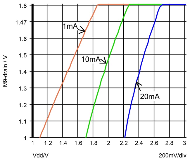
Figure 16-12. Dropout voltage of the circuit in Figure 16-11.
The circuit was designed for a supply voltage of 3 to 3.6 V and a regulated output of 1.8 V. It achieves an adequate phase margin with Rext, as Figure 16-13 shows.
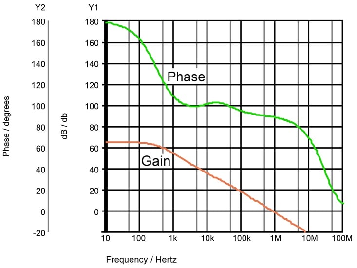
Figure 16-13. The CMOS regulator in Figure 16-11 has an adequate phase margin.
However, as illustrated in Figure 16-14, Rext limits power supply rejection at high frequencies.
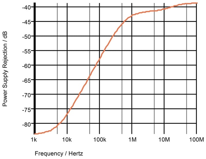
Figure 16-14. Power supply rejection.
Frequency compensation is nearly as difficult as in the previous example. An external capacitor with a resistor in series is again necessary at the output to create a zero and turn the phase up.
Regulator With an External PNP Transistor
The last linear regulator we'll look at (Figure 16-15) makes the most sense for higher-current applications.
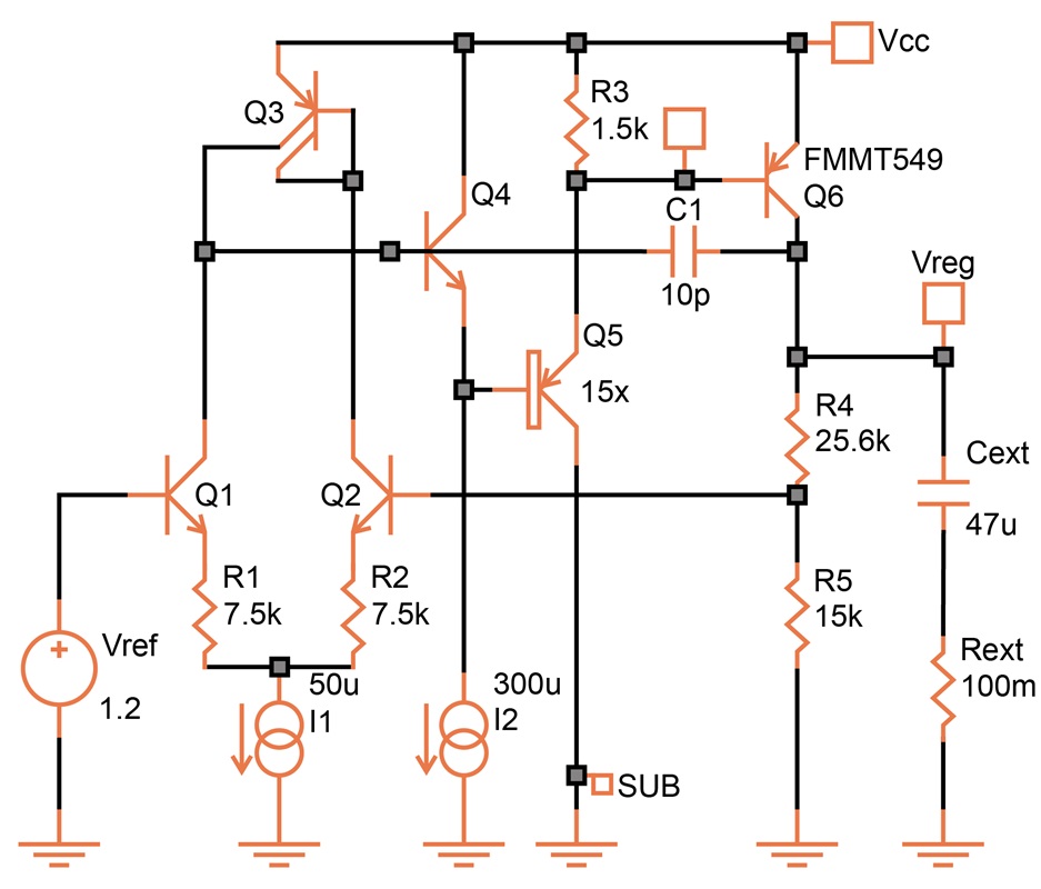
Figure 16-15. [click to enlarge] Low-dropout regulator with an external PNP transistor.
This regulator uses an external PNP power transistor. It requires an extra pin, but it greatly reduces the area and power dissipation of the IC. Also, depending on the external transistor used, the dropout voltage can remain low even at high current.
Using an FMMT549 for Q6, the maximum current is around 500 mA. At this level, the supply voltage can drop to within 200 mV of the output (3.3 V). This is illustrated in Figure 16-16.
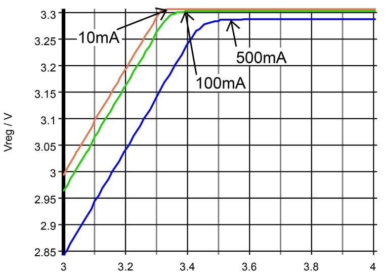
Figure 16-16. Dropout voltage.
There is, however, a compromise in the loop gain, which affects the output impedance (33 mΩ). In order to achieve stability, the gain has to be reduced using R1 and R2. Also, as in the two previous circuits, an output capacitor with a resistor in series is required to keep the phase from reaching zero before the gain does. Figure 16-17 shows the phase margin of this circuit.
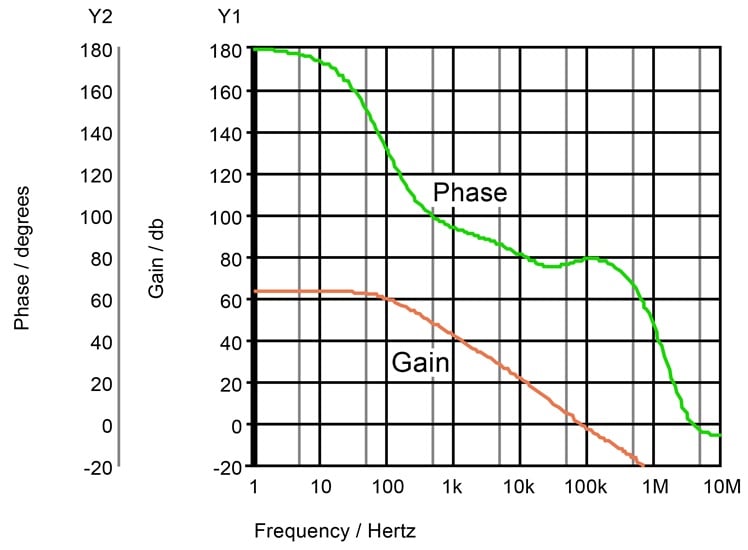
Figure 16-17. Phase margin can only be kept high by a resistor in series with the output capacitor.
This scheme again impairs power supply rejection at high frequencies, as shown in Figure 16-18.