Facebook
 Google
 GitHub
 Linkedin
Linear Power Amplifiers
A Class A amplification stage (such as the output of the bipolar op amp we introduced in a previous chapter) has a steady DC current through the transistor. In the extreme, this current can be varied between zero and twice the idle value.
The power efficiency of such a stage is dismal. A Class A amplifier can only reach 50% at maximum output, and with smaller signals the efficiency is much lower. In ordinary amplification, we usually don't care about efficiency. When it comes to a power output stage, however, Class A is ill-suited.
A Class B amplifier uses two output devices: one for the positive-going signal and one for the negative half. There is no idle current. Instead, each device starts to conduct as soon as the signal crosses the zero threshold.
This is an idealized concept that doesn't really work in practice. It's very difficult to switch from one device to the other without either leaving a gap or having both devices conduct at the same time. The result is distortion, which becomes very noticeable at low signal levels.
The solution is a compromise: allow a small idle current so that the amplifier works in a Class A mode with small signals and gradually moves to Class B as the signal increases. This operation is called Class AB. Such an amplifier is shown in Figure 16-29.
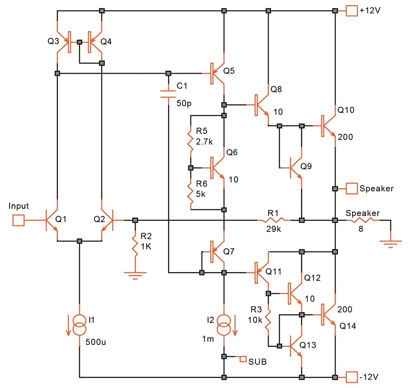
Figure 16-29. [click to enlarge] 5 W bipolar Class AB amplifier.
The two output devices in Figure 16-29 are Q10 and Q14. They are large, having an effective emitter length some 200 times that of a minimum-geometry transistor.
Ideally, we would want one of the two output devices to be a PNP transistor so that we can exploit the complementary nature of the push-pull output. But NPN transistors typically carry a much higher current than PNP ones. With a 5.8 W output capability (requiring peak currents of 1.2 A) this is no minor consideration.
To deliver the high output current, the upper stage (Q8, Q10) uses a Darlington configuration. Q9 serves to bypass leakage current at high temperatures.
The lower output stage has an identical Darlington connection (Q12, Q14) plus a PNP transistor (Q11). The entire four-transistor block behaves like a PNP transistor. All PNP transistors in this circuit are fairly large, capable of carrying 3 mA.
There are three base-emitter junctions between the base of Q8 and the base of Q11. The current I2 and transistors Q6 and Q7 generate a voltage between these two nodes. This voltage causes a few hundred microamperes of idle current to flow through the two output transistors. The VBE of Q6 is increased with the resistor divider R5/R6 to the point where the desired current is reached. Notice that Q6 tracks the base-emitter voltages of Q8 and Q10. Similarly, Q7 tracks the VBE of Q11.
The feedback resistors R1 and R2 set the gain at 30 dB, while C1 provides frequency compensation. The slowest device in the amplifier is the compound PNP transistor Q11 to Q14, but it is fast enough to allow a more than sufficient frequency response for an audio amplifier without creating stability problems (Figure 16-30).
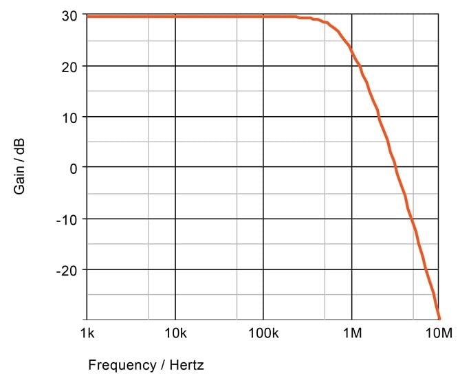
Figure 16-30. Frequency response of the Class AB amplifier.
One significant drawback of using only NPN power devices is the voltage drop. Only ±10 V are available at the output from the ±12 V power supply without creating distortion. At 10 V (Vpeak), however, the distortion amounts to only 0.15%. The spectrum of the output voltage is illustrated in Figure 16-31.
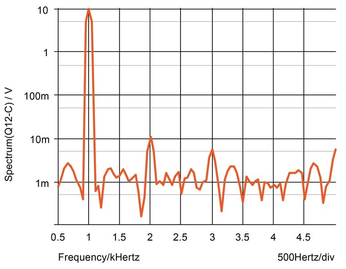
Figure 16-31. Spectrum of the output signal at full power.
The maximum efficiency of an ideal Class B amplifier is 76%. For this circuit, with its 2 V drop in each output device, the maximum efficiency amounts to 62%. The output transistors thus produce 1.7 W of heat each for a 5.6 W output.
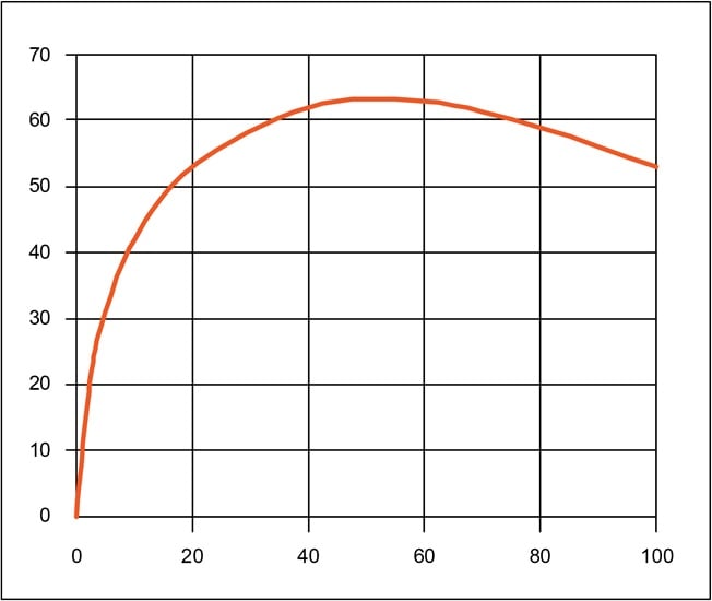
Figure 16-32. Power dissipation vs. power output in a Class B amplifier.
When it comes to audio applications, it's often argued that peak power is rarely required and so the heat sink for the amplifier can be reduced in size. Unfortunately, in a Class B (or AB) amplifier, peak dissipation occurs not at peak output, but at about 50% of maximum power. The design of Figure 16-29 requires a split power supply.
There are two ways to avoid this. One is to convert the –12 V connection to ground, make Vcc 24 V, bias the input at 1/2 Vcc and couple the speaker through a capacitor. The only problem with this approach is the size of the new capacitor: 2000 μF to get a 3 dB drop-off at 10 Hz.
A better solution is the bridge output (Figure 16-33). In essence there are two amplifiers, 180 degrees out of phase. With no input signal, both outputs rest at 1/2 Vcc. As the signal appears, one output moves up, the other one down.
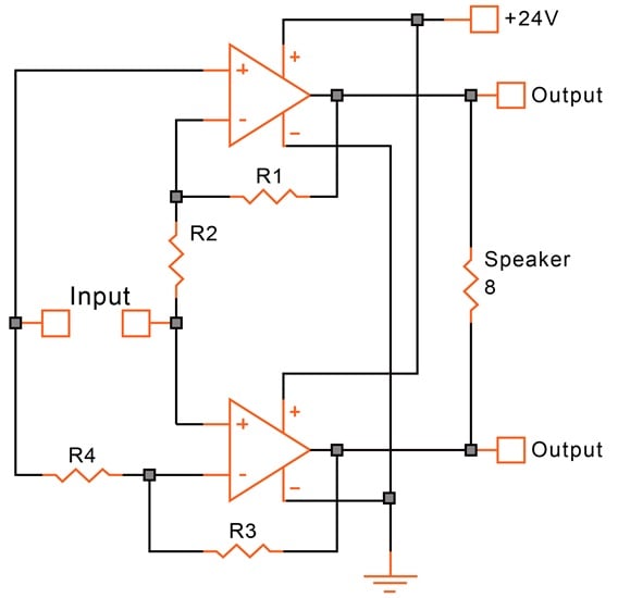
Figure 16-33. Class AB amplifier with bridge output.
In this configuration, we have actually doubled the output swing. The same total supply voltage generates 25 W of output (which requires four output transistors with a capability of 2.5 A each). Efficiency is unchanged at 62%, which produces a power dissipation of 15.3 W.