Facebook
 Google
 GitHub
 Linkedin
Linear Regulators
Let's say you have a car battery with a 12 V output, but you need 3.3 V. The 12 V source fluctuates between 10 and 14 V. Your 3.3 V load consumes up to 500 mA and needs to be regulated within 5%.
The immediate choice to effect this change in voltage is a linear regulator. Look at it as a variable resistor, dropping whatever voltage is not needed. Figure 16-1 provides an example.
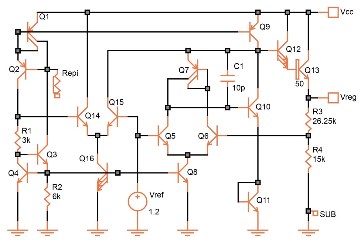
 Figure 16-1. [click to enlarge] Linear regulator with NPN power stage.
The unwanted voltage is often dropped in an NPN transistor. In Figure 16-1, this is a Darlington configuration to minimize the drive current. It requires at least 2.2 V difference between Vcc and Vreg, but it is an easy and simple design.
The regulator uses a 1.2 V bandgap reference whose voltage is compared with a fraction of the regulated output by the differential amplifier (Q5, Q6, Q7, and Q10). Once the circuit is in balance, the voltages at the bases of Q5 and Q6 are equal. The regulated voltage is therefore:
$$V_{reg} ~=~ \frac {V_{ref}{(R_3~+~R_4)}}{R_4}$$
An operating current is set up by Q1 to Q4 (a circuit derived from the ΔVBE current source in Chapter 6). This current is mirrored by Q9. At this point, we have about 150 μA.
The operating current has a deliberate negative temperature coefficient. R2, which creates this current, is connected across a VBE, which itself has a negative tempco. This counteracts the positive tempco of hFE.
Q10 shunts to ground whatever operating current is not needed by the output stage. Using a Darlington configuration for the output greatly reduces the required operating current, but there must always be a substantial voltage drop between supply and output. For this reason, as shown in Figure 16-2, such a circuit is anything but a low-dropout regulator.
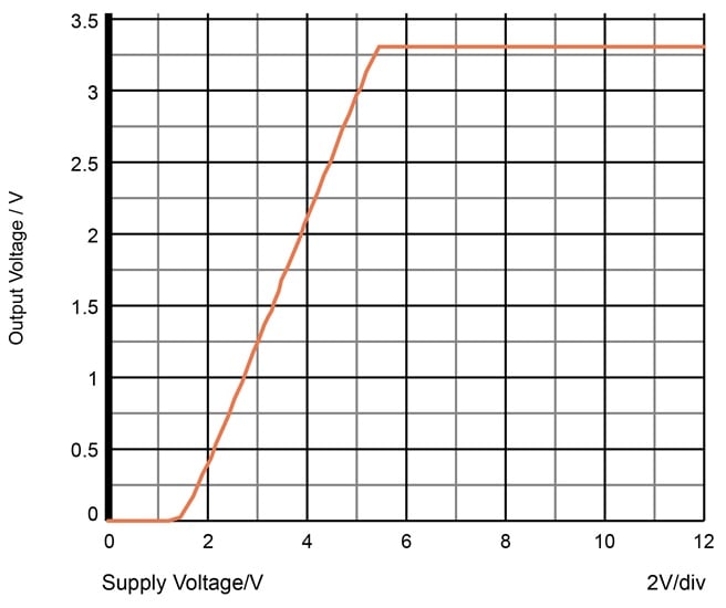
 Figure 16-2. Dropout voltage of an NPN regulator.
For our application, a conversion from 10 V minimum to 3.3 V, the voltage drop is of little concern.
Power Dissipation
The current that flows through the load also flows through the output transistor. So, at 500 mA, the load consumes 1.65 W, and the regulator consumes 4.36 W at 12 V, which is simply converted into heat. Figure 16-3 shows the linear regulator's power dissipation.
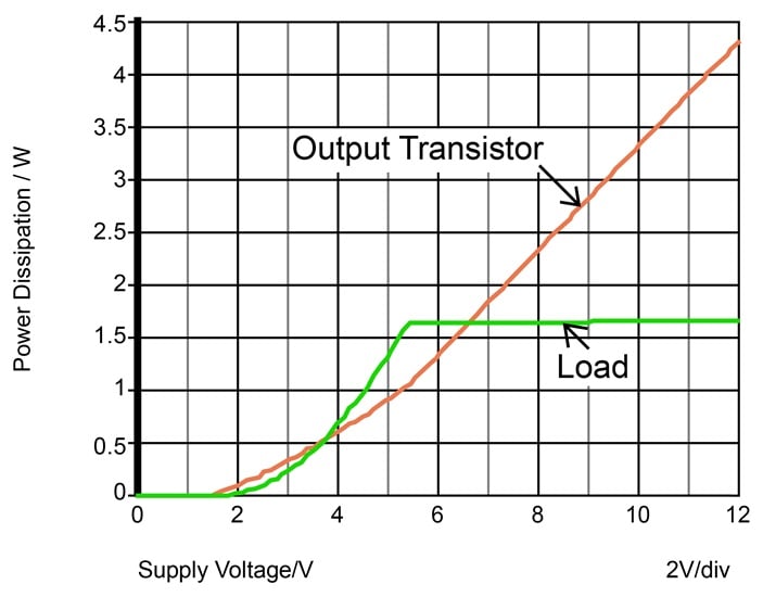
 Figure 16-3. In a linear regulator, the energy not required by the load is converted into heat.
This power dissipation is the main disadvantage of a linear regulator. The heat is produced mainly by one device: Q13. Even with an adequate heat sink, there will therefore be a hot spot on the chip that results in temperature gradients. These temperature gradients are bound to influence other circuitry on the chip, including the regulator's own reference.
Compensating the Linear Regulator
A linear regulator with an NPN output transistor is relatively easy to compensate. Despite the fact that the loop gain is high, which results in an output impedance of a mere 4 mΩ, the circuit is rendered stable with a single 10 pF compensation capacitor. This is illustrated in Figure 16-4.
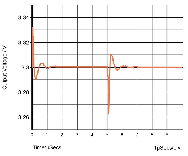
 Figure 16-4. The regulator is stable, even with a filter capacitor at the output.
Because of the low output impedance, it takes a massive capacitor at the output to have an effect of power supply rejection (Figure 16-5).
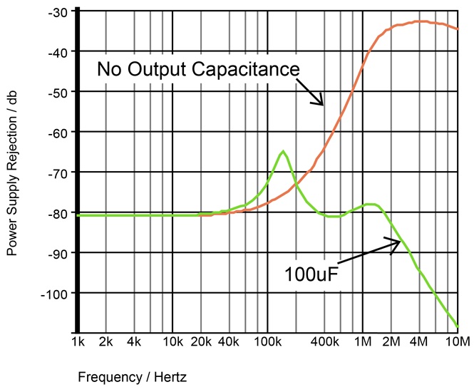
 Figure 16-5. Power supply rejection with and without a filter capacitor.
There are three transistors and a resistor in this design which we haven't discussed yet. The differential pair Q14/Q15 compares the reference voltage (which is assumed to have a very small temperature coefficient) with a voltage slightly higher than 2VBE (which has a strong negative tempco).
At temperatures below about 120 °C, the voltage at the base of Q14 is higher than Vref, and Q15 is cut off. But at about 140 °C, these two voltages become equal, and Q15 diverts the operating current for the output stage. Thus, when the chip gets too hot, the output collapses and the source of the heat disappears. This makes the regulator virtually indestructible.
As the Monte Carlo analysis in Figure 16-6 indicates, the accuracy of the shutdown point is ± 10 °C.
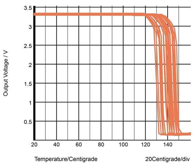
 Figure 16-6. Temperature shutdown.