Facebook
 Google
 GitHub
 Linkedin
Switching Regulators
Assume again that you have a supply voltage of 12 V, but you need 3.3 V. Your load consumes 1 A. A linear regulator acts as a resistor which drops the unneeded 8.7 V. In the process, it converts 8.7 W into heat. Only 3.3 W is used by the load, which is a rather dismal efficiency.
Enter the switching regulator (Figure 16-19). Instead of creating a resistance between input and output, it connects an inductor between the two for short periods of time.
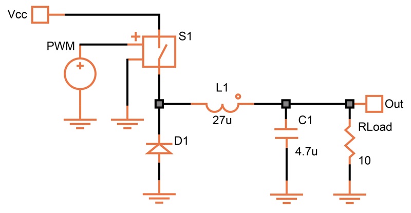
Figure 16-19. Reducing a supply voltage with a series switch and inductor.
The switch, S1, is driven by a pulse-width modulator (PWM). The pulses are rapid, so that the inductor value can be small. The inductor, together with C1, smoothes out the switching pulses.
Assuming the switch has no resistance, the left node of the inductor is at Vcc when the switch is closed. When the switch opens, this voltage jumps abruptly to a large negative value, created by the energy stored in the inductor. It is the purpose of D1 to catch this negative spike so it does no harm to the switch and provides a path for the current during the OFF period. Figure 16-20 shows the resulting waveform at the output for duty cycles of 10%, 20%, and 40%.
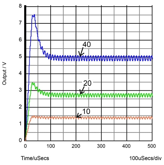
Figure 16-20. The resulting waveform at the output.
The average output voltage is simply proportional to the duty cycle. However, there is a noticeable ripple. This is the remainder of the switching frequency (100 kHz). There is also an overshoot, which becomes more pronounced as the duty cycle increases. This undesirable behavior is due to the LC filter (L1, C1).
With ideal components, the voltage conversion is 100% efficient. But when you add some resistance to the switch and inductor and a forward voltage drop for the diode, the efficiency drops. For example, with a total resistance of just 50 mW and a Schottky diode drop of 0.3 V, the efficiency is 94%.
Buck Regulators
The circuit of Figure 16-19 is not a regulator. We have to add feedback to make the output voltage immune to supply fluctuations. This is accomplished by amplifying the difference between a fraction of the output voltage (R1, R2) and a reference voltage in an error amplifier. Such a circuit is generally called a buck regulator.

Figure 16-21. Buck regulator.
S1, an abstract simulation symbol, is now used as both a switch and a comparator (with the ON/OFF thresholds set just a few millivolts apart). The output of the low-pass filter (R3, C2) following the error amplifier is thus compared with a triangle wave (100 kHz, 2Vpp). In this way, the regulator finds the duty cycle which gives the desired output voltage. Figure 16-22 shows the response as the regulator output stabilizes over time.

Figure 16-22. Output voltage vs. time.
Design Considerations for Switching Regulators
Let's use the buck regulator to examine a few considerations peculiar to switching regulators.
First, an actual switch is not a perfect device. You will have to make a painful compromise between voltage drop and speed: the lower the voltage drop, the more current it takes to drive the device. For example, a discrete MOS transistor with an ON-resistance of 100 mW at 1 A has a total input capacitance of about 1 nF. At a switching frequency of 100 kHz, you'll need to turn the device ON and OFF in less than 50 ns. Otherwise, the dissipation during switching will become significant.
This means the output of the comparator (the driver stage) has to provide 100 mA to charge and discharge 1 nF. If you push the switching frequency to 500 kHz, this current increases to 0.5 A.
Second, the current level that the switching transistor needs to handle is always larger than the average output current. If you use a small inductor, the peak current can exceed the average by a factor of three or more. With a large inductance, this factor is between 1.1 and 1.4.
Third, the voltage drop (and switching speed) of the diode is just as important as that of the switching transistor. Their peak currents are roughly equal.
Fourth, the output LC filter (L1, C1) forms a pole, which makes frequency compensation (R3, C2) more challenging.
We can step up the voltage by using the induced voltage in an inductor. In Figure 16-23, switch S1 connects the inductor L1 across the power supply (here assumed to be 1 V).
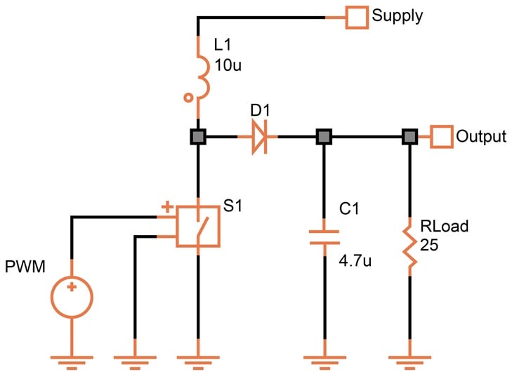
Figure 16-23. By using inductive charge, the output voltage can be made higher than the supply voltage.
The current flowing through the inductor is given by:
$$I ~=~ \frac {V~\times~t}{L}$$
As soon as the switch is turned OFF, a positive voltage appears at the anode of the diode, created by the stored current. This voltage is averaged by C1.
The magnitude of the output voltage depends on how long the inductor is charged (in other words, what peak current is reached). Thus, by changing the duty cycle, the output voltage is altered. This is shown in Figure 16-24.
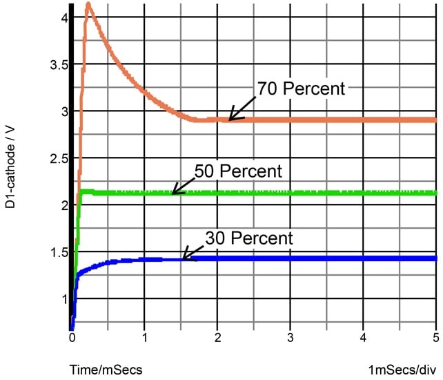
Figure 16-24. Output voltage for three different duty cycles.
Note that in this configuration, too, the switching device must handle a current that's considerably larger than the output current. We can see this in Figure 16-25, which plots both the switch current (the orange curve) and the output current (the green curve).
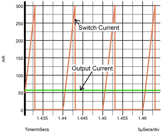
Figure 16-25. Currents through switch and load.
Boost Regulators
Add feedback and we have a boost regulator (Figure 16-26).
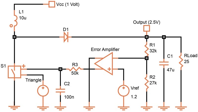
Figure 16-26. Boost regulator.
As before, the switch symbol represents both the switch and a comparator. The switch turns ON and OFF within a few millivolts of the differential input signal. Be aware that, in this configuration, the output of the error amplifier must be constrained so that it stays within the amplitude of the triangle waveform. Otherwise, the regulator can hang up at either zero or full output.
As shown in Figure 16-27, the frequency compensation network (R3, C2) also provides a soft start. This means that the output voltage builds up gradually, without much of an overshoot.
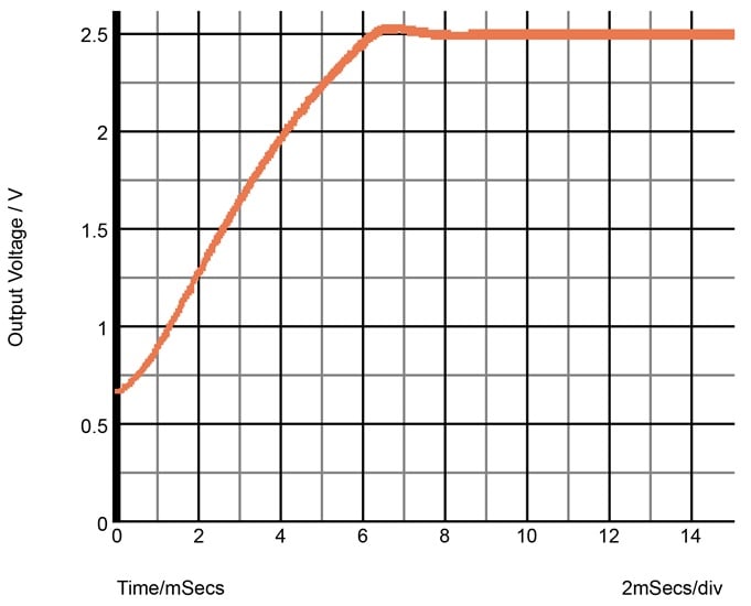
Figure 16-27. Soft start of the boost regulator.
The same principle of using the inductive "kickback" voltage is also used to regulate larger voltages (such as a 110 V or 220 V line input). The inductor becomes a transformer, with a secondary winding delivering a lower voltage that is isolated from the line. To provide isolation, an optical link (an LED and a phototransistor) is used to provide the feedback.
Some of the devices in such a line regulator, including the switching transistor, need to operate at high voltage. You need to be aware that this increases device size considerably, as we'll discuss below.
The Area Penalty for High-Voltage Devices
As we learned in Chapter 2, depletion layers take up space. The higher the operating voltage, the wider the depletion layer. The diffusions need not only to be deeper, but also more widely spaced.
Just how serious is the penalty of using large voltages in an IC? Take a look at Figure 16-28. It compares the required areas for minimum-geometry bipolar transistors operating at 5, 20, 40, and 100 V.
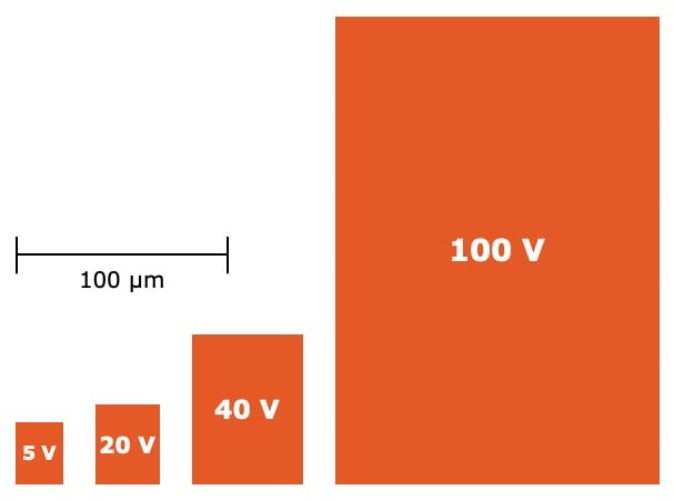
Figure 16-28. Minimum areas for bipolar transistors at different operating voltages.
| Max Voltage | Dimensions (μm) | Area Ratio |
| 5 | 22 × 29 | 1.0 |
| 20 | 30 × 37 | 1.7 |
| 40 | 52 × 70 | 5.7 |
| 100 | 152 × 220 | 52.4 |
If only a small portion of the circuitry is required to withstand a high voltage, you wouldn't want all of the devices to pay the price of large dimensions. This then calls for a more complex process, one capable of producing both shallow, narrow devices and deep, wide ones.