Facebook
 Google
 GitHub
 Linkedin
Switching Power Amplifiers
The goal of the switching power amplifier is almost the same as that of the series switching regulator: lower a voltage across a load without creating much heat. However, it differs in that the output starts at zero and can move in either the positive or negative direction.
To start with, let's use two power supplies to build a switching power amplifier. In Figure 16-34, the two switches connect the inductor to either the positive or negative rail. For now, we assume that there is no dead time or overlap and that this switching action is instantaneous.
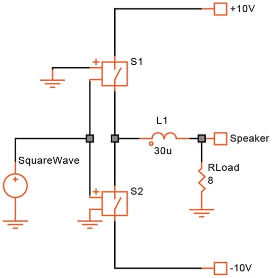
Figure 16-34. Bidirectional switching arrangement.
The value of the inductor is fairly large for the chosen switching frequency (200 kHz). It is never fully charged or fully discharged. Despite this, we see in Figure 16-35 that there is still a substantial ripple at the output.
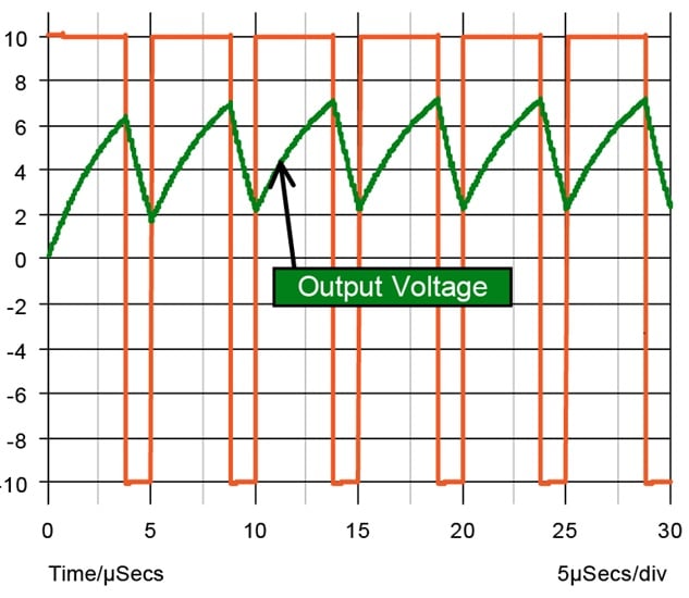
Figure 16-35. Switching and output waveforms.
The average output voltage is a function of the duty cycle. Duty cycles of less than 50% cause the output to be negative. At 50%, the output is zero; at 75%, it is +5 V. A 100% duty cycle produces +10 V.
In Figure 16-36, you'll notice that the current gradually builds up. The time constant of this effect is given by L1 and the 8 Ω load (a speaker), a factor which will become important when we close the loop with feedback.
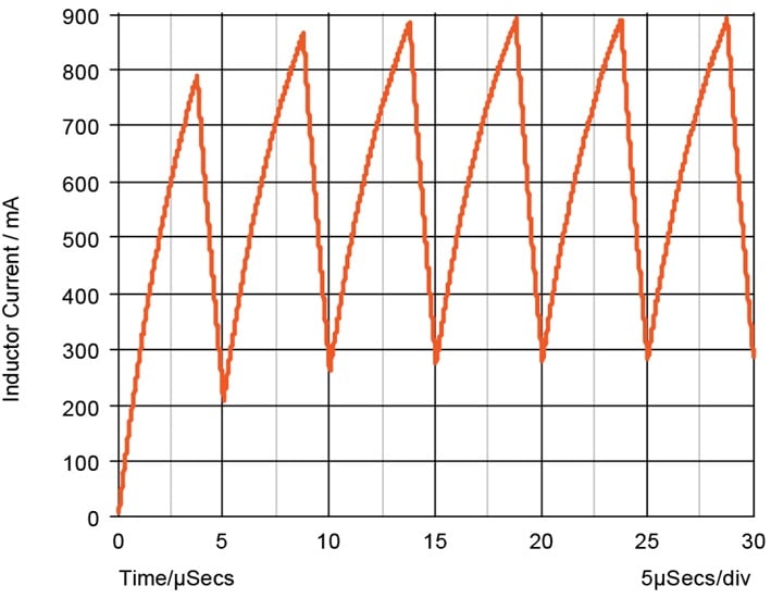
Figure 16-36. Current through S1.
Class D Amplifier
Let's now take the next step and modulate the duty cycle with a sine-wave signal, making a Class D amplifier (Figure 16-37).
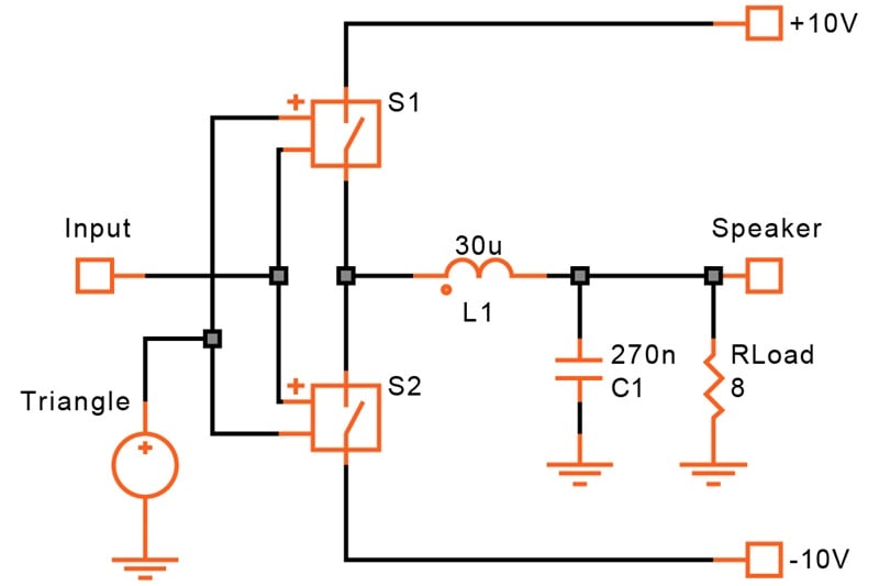
Figure 16-37. Class D amplifier.
As in the switching regulators, the switches also act as comparators. The thresholds of the control terminals are set so that the switches turn from OFF to ON (and from ON to OFF) within a few millivolts. We're assuming for now that the switches are ideal, so they have no delay and insignificant resistance.
A filter capacitor (C1) has also been added. This reduces the 200 kHz ripple, but increases the build-up delay mentioned above. The output (Figure 16-38) is now a sine wave with a small amount of 200 kHz ripple.
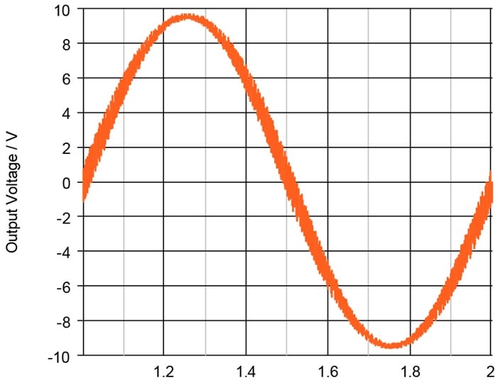
Figure 16-38. Output waveform.
As shown in Figure 16-39, the distortion is very small because we're using near-perfect components.

Figure 16-39. Frequency spectrum in the signal range.
The high-frequency switching creates noise at frequencies above the signal bandwidth of interest (Figure 16-40).
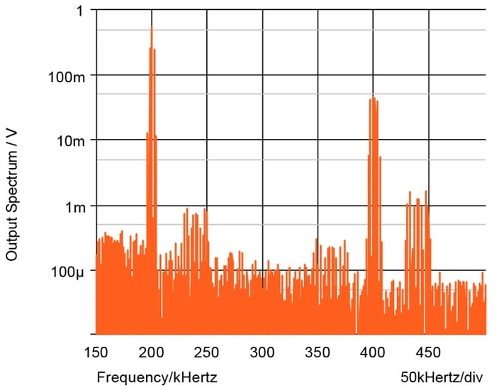
Figure 16-40. Frequency spectrum in the switching range.
The Limitations of Non-Ideal Components
Alas, if we only had ideal components. In reality, the switches have resistance and significant switching times. In addition, as pointed out in our discussion of switching regulators, they require painfully large amounts of drive power. In Figure 16-41, the models are changed to represent more practical components.
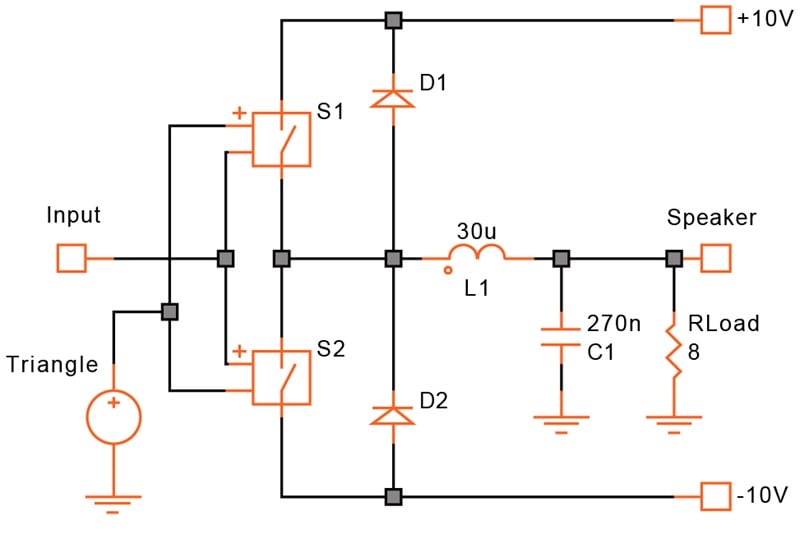
Figure 16-41. Pulse-width modulated circuit with more practical component models. The diodes are now required to absorb the voltage spikes.
The switch resistances in Figure 16-41 result in larger, unequal voltage drops (200 mV for an N-channel transistor, 300 mV for a P-channel one). In addition, there is a small dead time to avoid both devices being ON at the same time. This dead time creates a voltage spike from the inductor, which makes D1 and D2 necessary.
These small imperfections have a significant impact on the fidelity of the output signal. As shown in Figure 16-42, distortion increases to 1%.
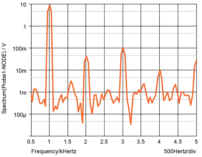
Figure 16-42. Signal spectrum with realistic components.
Unless we use faster-switching transistors with lower voltage drops and better matching, the level of distortion can only be brought down with feedback. This is something of a problem.
In order to reduce the high-frequency components at the output we used an LC filter. It is dimensioned to be effective at 200 kHz, but it causes a phase shift already in the audio range (Figure 16-43). Because of this, the amount of feedback possible using a single feedback loop is limited to about 20 dB. With two or even three nested feedback loops, this increases to about 35 dB.
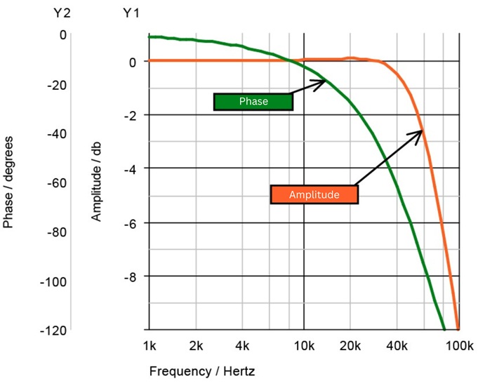
Figure 16-43. Amplitude and phase response of the output filter.
Also, a loudspeaker is not really a simple resistor. There is some inductance as well, making the phase relationship in the feedback path even more complicated.
We could, of course, increase the switching frequency, which would allow us to push the cutoff frequency of L1 and C1 higher, but the penalty would be lower efficiency and an increase in drive requirements for the switching transistors.
Practical Issues
We have been assuming that we want a faithful (albeit larger) reproduction of the input signal at the load. Strictly speaking, this is not really true. In the case of an audio amplifier, the human ear cannot hear 200 kHz, so filtering out high frequencies makes little difference. If the application is a servo amplifier, the load is unlikely to respond to such rapid fluctuations.
But there is radiation. Do we want to connect a square wave of 200 kHz (and its harmonics) across a long speaker cable and let it radiate into AM receivers and other electronic equipment? The answer is a clear no, and rules and regulations limiting such radiation have been written.
There are ways to reduce radiation. First, we can keep the speaker wires short, moving the amplifier next to the speaker. Second, we can vary the switching frequency in a random fashion, creating a spread spectrum. Although this does not reduce the total radiation, it at least makes it less noticeable and allows meeting radiation limits.
Bridge Output for Increased Power
For a given supply voltage and speaker impedance, the delivered power can be increased by using a bridge output, as in Figure 16-44.

Figure 16-44. [click to enlarge] Class D amplifier with bridge output.
In Figure 16-44, there are four switches. S1 and S4 are always ON and OFF together, as are S2 and S3. The load is therefore either connected to +V on the left side and –V on the right, or vice versa. This effectively doubles the supply voltage; the amplifier can deliver 25 W into an 8 Ω load. There are four large output transistors, however, each of which must carry up to 2.5 A.
If we apply 40 V total and use a 4 Ω speaker, the output power grows to 196 W (and the peak current in the four output devices to 10 A).
Differential Drive
But now let's change the circuit a little. Instead of having the two outputs move in opposite directions, we invert one of the drives so that they move up and down together (Figure 16-45).
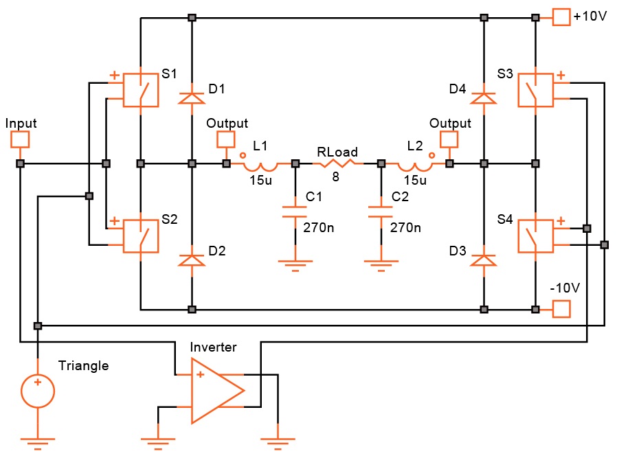
Figure 16-45. [click to enlarge] Class D amplifier that suppresses the fundamental of the switching frequency.
If the input signal is zero, the two outputs will move at exactly the same time. Each output then carries a 200 kHz square wave, but between them there is no signal. As the input signal goes positive, the duty cycle of one output increases. Meanwhile, the duty cycle of the other output decreases by the same amount. Thus, between the two outputs, there is now a square wave with a duty cycle amounting to the difference.
The effect on the frequency spectrum is quite drastic: the fundamental of the 200 kHz switching frequency has disappeared (Figure 16-46). We only need to worry about the second harmonic at 400 kHz, which has a lower amplitude and is easier to filter out.
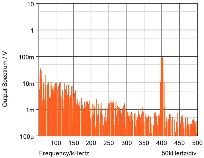
Figure 16-46. Radiation spectrum across the load in Figure 16-45.
But let's not get too enthusiastic here. The fundamental of the switching frequency is no longer present when measured across the load, but the wires leading to the load move up and down together at the rate of the switching frequency. While this movement causes no current to flow through the load, there is still capacitive radiation from the wires. This is why C1 and C2 are needed.
Final Thoughts
A last word about Class D amplifiers: simulation is very difficult and time-consuming. Unless you have a highly specialized program, only transient analysis can be used, which means you cannot obtain such parameters as phase margin directly. You may be forced to simulate (and integrate) the various blocks in pieces and then resort to old-fashioned breadboarding.