Facebook
 Google
 GitHub
 Linkedin
Connections and Metal Routing
Bipolar analog ICs can often be connected using a single metal layer, which lowers the cost. However, you will inevitably find spots where two metal lines need to cross.
Alternatively, we can use the diffused layer with the lowest resistance (N+ emitter) as an additional routing layer. To achieve this, the interconnection stops at a contact, dives under the second metal line, and continues at the second contact. This introduces a small amount of resistance (about 20 Ω), which is tolerable in places with low current, like the base of a transistor.
Figure 19-15 shows one way of creating a cross-under. The N+ rectangle is placed inside a base diffusion, which itself sits inside an epi-island. One side of the cross-under is connected to the base region. It doesn't matter which side, since the voltage drop across the cross-under is bound to be much smaller than that of a diode.
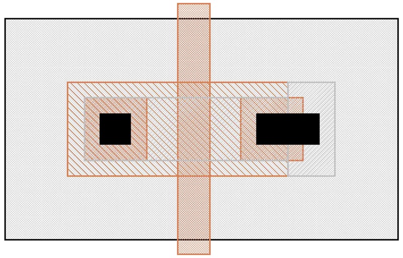
Figure 19-15. N+ cross-under.
If the epi-island is biased at the highest positive supply voltage, you can have several such cross-unders in the same island.
The epitaxial region can serve as a cross-under as well, though it takes up more space.
The NPN transistor with two collector contacts (Figure 19-16) is a special case of using the diffused layer for routing. Here, a line connected to the collector stops at the right-hand contact and continues on at the left-hand one.
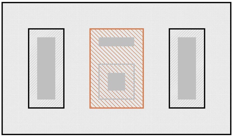
Figure 19-16. Two collector contacts in an NPN transistor can act as a cross-under.
Be careful with this scheme, however. Let's assume the resistance between the contacts is 100 Ω. The resistance between one contact and the center point underneath the emitter is then about 50 Ω. If one contact carries all or most of the collector current, the second contact will reflect the voltage at the center and not that of the first contact.
Kelvin Connections
Any contact on the surface of an IC has some resistance, which often makes precision measurements difficult. This can be avoided by providing two sets of contacts—one to carry the current and the other to measure the voltage. Figure 19-17 shows such a setup, which is known as a Kelvin connection.
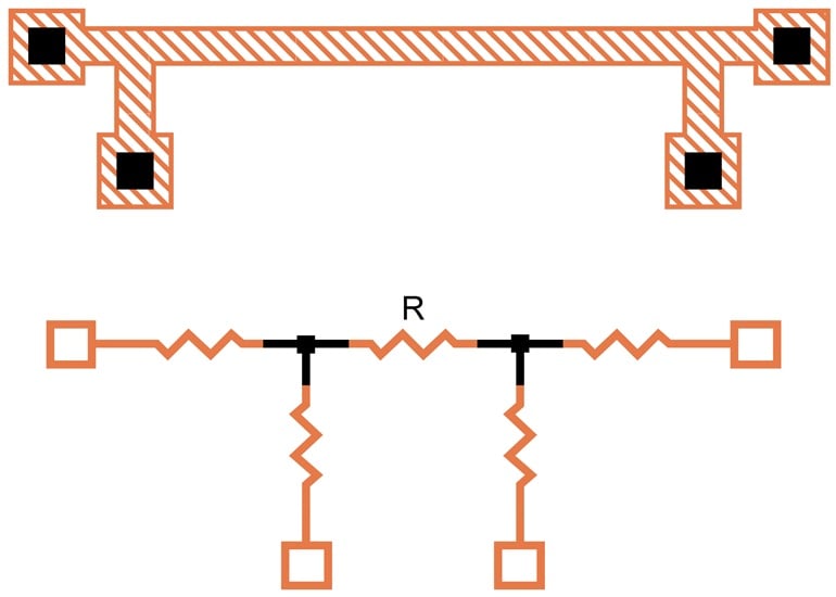
Figure 19-17. A Kelvin connection for a resistor and its equivalent circuit.
In a Kelvin connection, contact resistance is of no consequence. The two resistances in the current path add a bit to the headroom required, while the two in the measurement path simply need to be negligible compared to the measuring impedance.
Metal Runs and Ground Connections
The concept of an analog ground is often misunderstood. It is meant to be a noise-free point that can be used as a 0 V reference. Analog grounds can be found either on a circuit board or an IC.
The usual practice designates a pin that carries little or no current as the analog ground. Other pins, intended to be at the same potential but carrying current, are then connected to this point on the circuit board.
There is another way to achieve this, one that both saves a pin and has better performance. A package pin has low resistance—lower than a trace on a circuit board or a metal run on the IC. Designate a pin as the analog ground and then connect two neighboring pads to it with separate bonding wires. One path carries no current and serves as the analog reference ground on the IC; the other carries the potentially polluting currents.
Similarly, on the IC, use separate metal runs to connect sensitive devices. Figure 19-18 shows the right and wrong way to do this.
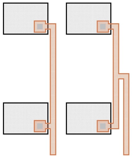
Figure 19-18. Proper connection (on the right) and improper connection (on the left) for matching devices.
In this figure, the left-hand connection can create an error. For example, say that the runs lead to emitters carrying 1 mA. With 50 squares (at 30 mΩ/□) of additional aluminum for the upper device, the voltage drop is 1.5 mV. This creates a current mismatch of 6% at room temperature. The balanced connection on the right avoids this problem.
Back-Lapping and Gold-Plating
To fit into small, shallow packages, wafers are often thinned down by back-lapping. This is a wet, grinding, and somewhat messy operation. It removes not only the oxide layer on the back but any diffusions which may have taken place there, giving direct access to the substrate material.
If you add a gold-plating step, you get a low-resistance connection directly to the substrate.
Ordinarily such a connection is not essential, as the substrate is also contacted from the top. But if you have sinned and allowed high substrate currents, you may be able to suppress the resulting effects in this way.