Facebook
 Google
 GitHub
 Linkedin
Improving Bipolar Op Amp Circuits
We previously evaluated a bipolar op amp design with NPN transistors as the input differential pair. Naturally, you can invert the polarity of the diff pair transistors by using PNP transistors. This allows the design of an op amp whose input can operate close to the negative supply (but loses its ability within about 1 V of the positive supply). Such a circuit is shown in Figure 10-10.
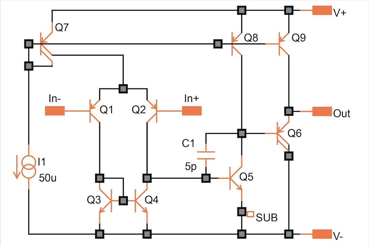
Figure 10-10. PNP-input equivalent of a three-stage op amp circuit. [click to enlarge]
Figure 10-10 is the PNP-input equivalent of Figure 10-1. It still has a rather primitive output stage (Q6, Q9). The output node can be pulled up to within about 150 mV of the positive supply (if the load does not require more than 50 μA), but only down to about 1 V above the negative rail.
The Folded Cascode Input Stage
Let's now consider Figure 10-11, a design in which the inputs can be operated all the way down to the level of the negative rail, and the output swings (almost) rail-to-rail.
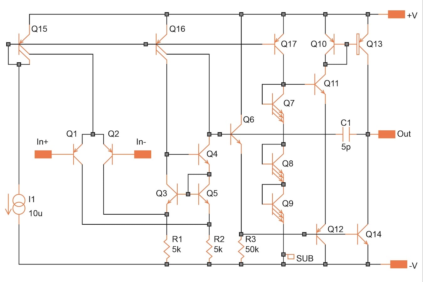
Figure 10-11. Op amp with folded-cascode input stage and (almost) rail-to-rail output. [click to enlarge]
The input stage in Figure 10-11 is a configuration known as the folded cascode stage. With an operating current (I1) of 10 μA, the voltage drop across R1 and R2 is a mere 50 mV. The inputs can therefore go about 250 mV below the negative supply rail without saturating Q1 or Q2. The collector currents of Q1 and Q2 upset the balance of the Wilson current mirror (Q3, Q4, and Q5), and the difference signal is picked up by Q6.
The output stage has two branches to it. The first one is simply NPN transistor Q14, a grounded emitter amplifier. All other transistors in this block serve its PNP opposite, Q13.
Note that transistors, Q7, Q8, and Q9 are diode-connected. They set a voltage for the base of Q11. If you follow the emitter-base junctions of Q11, Q12, and Q14, you’ll notice there are also three diodes in series to the V– rail. Because of this, the current in Q11 fluctuates as the input signal to the output stage moves up and down by a few mV. It is this current, amplified by the size ratio of Q13 to Q10 (here about 6) that becomes the pull-up portion at the output.
Q7 to Q9 are deliberately made larger than Q11, Q12, and Q14 so that the idle current in the output is small. This creates a small "dead-band." Because of the large loop gain, however, the distortion is very small: 0.0004% for a ± 4.7 V signal at 1 kHz.
In this circuit, we are fortunate to find a node ideally suited for the connection of a compensation capacitor to the output:
- At the base of Q6, the signal has a phase opposite to that at the output.
- The base of Q6 and the collectors of Q4 and Q16 all represent a high impedance.
- There is substantial voltage gain between the base of Q6 and the op amp output.
All of the above says that this op-amp can be compensated at unity gain with a single 5 pF capacitor, even though the loop gain is 110 dB. Not all designs behave that well.
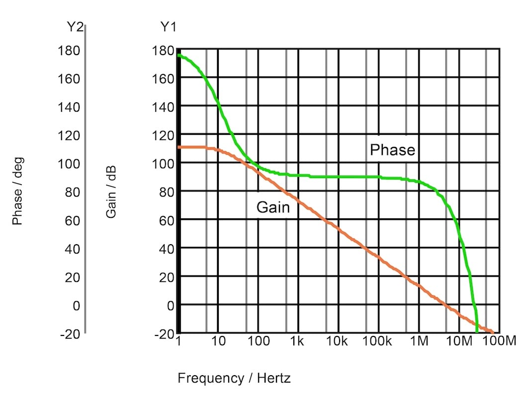
Figure 10-12. Gain and phase plots for the folded cascode amplifier showing roughly 70 degree phase margin. [click to enlarge]
Limitations of the PNP-Input Op Amp
Though the inputs can work at the level of V– (or ground, if you have only a single supply), the output cannot. It is the sad truth for a bipolar transistor that there is a saturation voltage. Unlike a MOS transistor, which is simply a voltage-controlled resistor, the bipolar transistor is the interaction of two junctions with different doping levels and sizes.
There’s a minimum voltage drop of about 150 mV between the emitter and collector in transistors Q13 and Q14 in Figure 10-11, even when they’re fully turned ON. The output can never be at the rails, only approach them. This is illustrated in Figure 10-13 by the slight flattening at the peak and trough of the sinusoidal waveform.
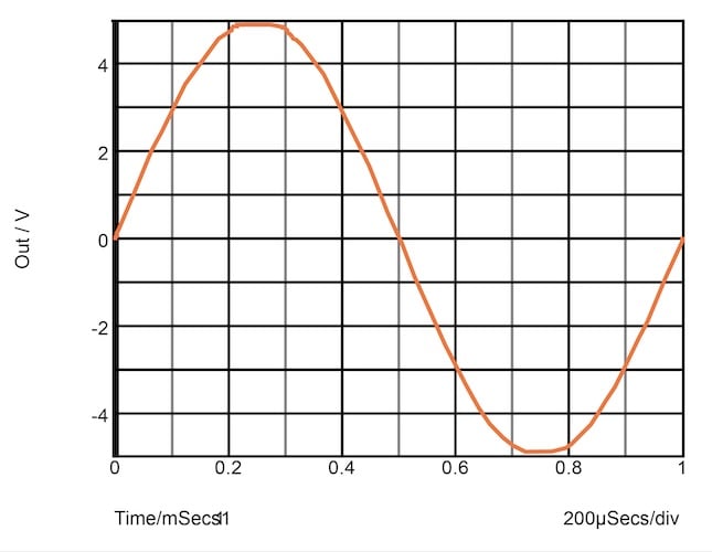
Figure 10-13. Output swing is limited by the saturation voltages of Q13 and Q14.
The use of lateral PNP transistors at the input and the low operating current are not kind to noise: 27 nV/√Hz at 10 kHz and up (white noise). At 1 Hz, the flicker noise rises to 80 nV/√Hz.
If you have vertical PNP transistors at your disposal and can afford a higher operating current, these figures drop by a large factor. However, you’ll need to carefully re-simulate the entire circuit, as its frequency behavior is bound to be entirely different.
Another unsatisfactory parameter of these bipolar op amps is the input current. Each input transistor runs at 5 μA. With a minimum hFE of 100 (in a good process), the base current can be as high as 50 nA. But there is a solution to this: more transistors.
Base-Current Compensation
In Figure 10-14, eight transistors are added. Their job is to pull as much current out of the bases of Q1 and Q2 as they require so that the external circuit doesn’t have to.

Figure 10-14. The folded cascode op amp modified with base-current compensation for the input stage. [click to enlarge]
The key to the base-current compensation is Q22. It’s identical in size and design to Q1 and Q2, has the same operating current, and is very close to the same collector-base voltage. The base-emitter voltage of Q23 and the diode-connected transistor Q24 set the collector-base voltage of Q22. Its base current is, therefore, the same as those of the input transistors.
The base current of Q22 is mirrored by Q21, Q20, and Q19. Transistor Q19 opposes the base current of Q1, while transistor Q20 opposes the base current of Q2. Ideally, the external circuit does not have to sink any of the base current from the input differential pair.
The cancellation of the base currents is never perfect, of course—the current levels are too small to get precise matching. However, the net input currents are down to 2 nA. That’s a 25:1 improvement.
Designing Op Amps for Low Noise
In the last bipolar op amp we’ll examine (Figure 10-15), the goal is not an ultra-low input current. Instead, we’re trying for low noise performance with a reasonably low input current.
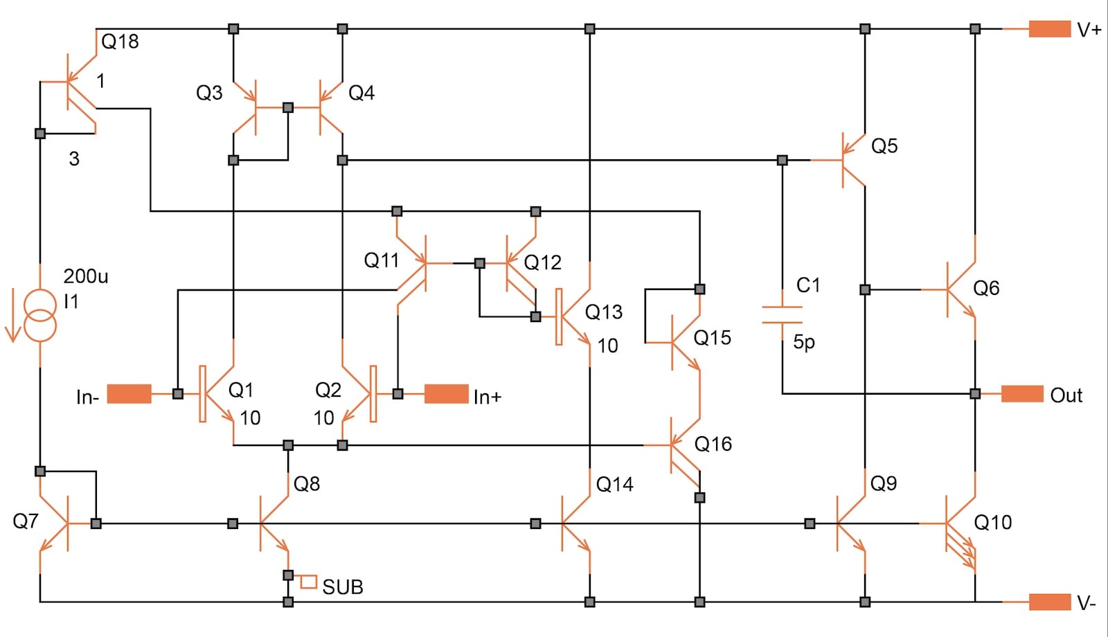
Figure 10-15. Bipolar op amp optimized for low noise. [click to enlarge]
This circuit is almost identical to the basic NPN-input op amp we saw in Figure 10-1. The input transistors are now again NPN, but with the base-current canceling scheme added.
The key transistor is Q13. Since the hFE of an NPN transistor changes much less with current than that of a PNP device, we can afford to run it at twice the current and then divide the base current by two in the current mirrors Q12/Q11. This brings the input current down to 20 nA.
The operating current is much higher than that of the previous circuit and the input transistors are large. This lowers the white noise to 5 nV/√Hz.