Facebook
 Google
 GitHub
 Linkedin
Triangle and Sine Wave Generators
Many circuits rely on the constant rising and falling slopes of a triangle wave for their operation. Other circuits require a more pure sine wave. Here, we’ll discuss the operation of a high-frequency triangle wave generator. Then, I’ll describe how we can modify the circuit to generate a sine wave output.
A High-Frequency Triangle Wave Generator
Figure 13-11 shows an oscillator that produces a precise triangle waveform even at relatively high frequencies. All transistors that determine speed are NPN and do not saturate.

Figure 13-11. A high-frequency triangle wave generator. [click to enlarge]
First, let’s consider the low-frequency part—the current sources used to charge and discharge the external capacitor, Cext.
The primary current is produced by Rext. The current through the resistor is dependent on the supply voltage because it is connected to the positive supply. This current also has a temperature coefficient because the voltage drop is also a function of two diode-connected transistor voltages (VBE). Both of these effects are eliminated by using an internal resistor chain (R9, R10, and R11) connected in the same way.
The primary current is mirrored by Q6, Q7, Q9, and Q10 and then mirrored again (Q1 through Q5) to form the charge current. A second current of twice the magnitude is derived from the first current mirror by Q8 and Q11. This second current is used to discharge the capacitor and is turned on and off by the differential pair Q13/Q14.
The internal resistor chain is used to bias the rest of the circuitry and provide the reference voltages for two comparators. The voltage across the three identical resistors is Vcc – 2VBE.
Comparator 1 consists of a single differential pair (Q18, Q21), as does Comparator 2 (Q23, Q25). They provide the operating current for the flip-flop (Q19, Q22) with two of their collectors while the other collectors switch the flip-flop's bases. The ratio of the resistors in this arrangement is key—the operating currents for the comparators are set by R12 and R13, which have one VBE across them.
The two currents end up flowing together through either R5 or R6, depending on the state of the flip-flop. R5 and R6 are one-quarter the value of R12 and R13, so the voltage drop across them is 1/2 VBE. In other words, the collector voltages of the flip-flop drop 1/2 VBE below the base potential. This amount is safely above the saturation voltage.
The challenge now is that:
- We have a small voltage fluctuation across R5 and R6 with a DC value just below Vcc.
- We need this fluctuation to drive the bases of the differential pair formed by Q13 and Q14.
- Q13 and Q14 must operate in the voltage region below the low point of the waveform.
- We can’t use lateral PNP transistors—they’re far too slow.
The solution is to couple the switching signal to the differential pair through two resistors (R3, R4) and run a known DC current through them.
Q12 and Q15 are current mirrors slaved to the bias chain (Q27). Their current thus increases as the supply is increased, and so do the voltage drops across R3 and R4. As a result, the average potential at the bases of the differential pair stays at a fairly constant 1/3 Vcc over an operating range of 9 to 15 V.
Figure 13-12 shows the triangle wave output created by this oscillator. The green line is the voltage fluctuation across R5, R6. The lower blue line shows the voltage fluctuations at the bases of Q13, Q14.

Figure 13-12. Triangle waveform generator operation at 1 MHz.
The triangle waveform across the capacitor is buffered by the emitter follower Q16 to drive both the comparators and an external load. At the unused collector of the differential switching pair, a square wave can be obtained.
This isn’t an oscillator of ultimate precision, but it delivers a good-quality waveform up to at least 1 MHz. The temperature coefficient is 190 ppm/°C, and the change in frequency from 9 to 15 V supply is 1.7%. As always, these results are based on one particular process—it’s a good idea to re-simulate the design for the process you’re using.
Shaping a Triangle Wave Into a Sine Wave
In many applications, we want to have a sinusoidal signal with a single frequency harmonic output. A triangle wave can be looked at as a sine wave with distortion. This distortion is only about 12%. If we round off the peaks, we end up with a fairly respectable sine wave with relatively little effort.
For example, we can use the circuit of Figure 13-13 as a companion circuit to Figure 13-11 to create a sine wave instead of a triangle wave. It is inserted between points A and B of that circuit, replacing R10.
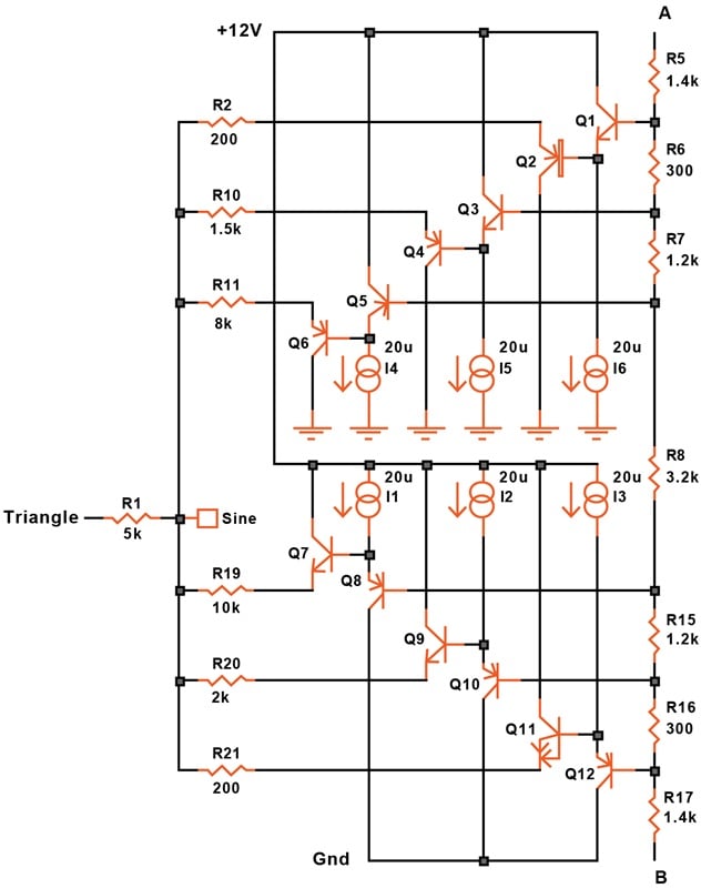
Figure 13-13. A shaping circuit that transforms a triangle wave into a sine wave. [click to enlarge]
The triangle wave enters through R1 and encounters attenuators at three voltage levels as it transitions from low to high and three voltage levels from high to low. Let’s examine an increasing signal to understand the circuit operation:
- At first, there is no attenuation.
- At about 0.6 V, R11 kicks in, held at that level by Q6.
- As the signal continues to increase, R10 appears in parallel to R11 and increases the attenuation.
- At the final level, an even smaller resistor, R2, reduces the signal even further.
Figure 13-14 shows the resulting sine wave.
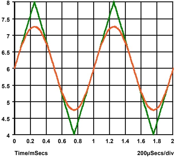
Figure 13-14. Triangle and sine wave.
With only three clipping levels in each direction, the sine wave has a distortion of only 1%. Using more levels reduces the distortion, but will likely require trimming.