
 Facebook
 Google
 GitHub
 Linkedin
The 555 Timer Revisited
Looking back 33 years later (in 2004), there are many areas where the original 555 timer shown in Figure 13-3 can be improved. We can use the design techniques we’ve learned since then and the enormous benefits of computer simulation.
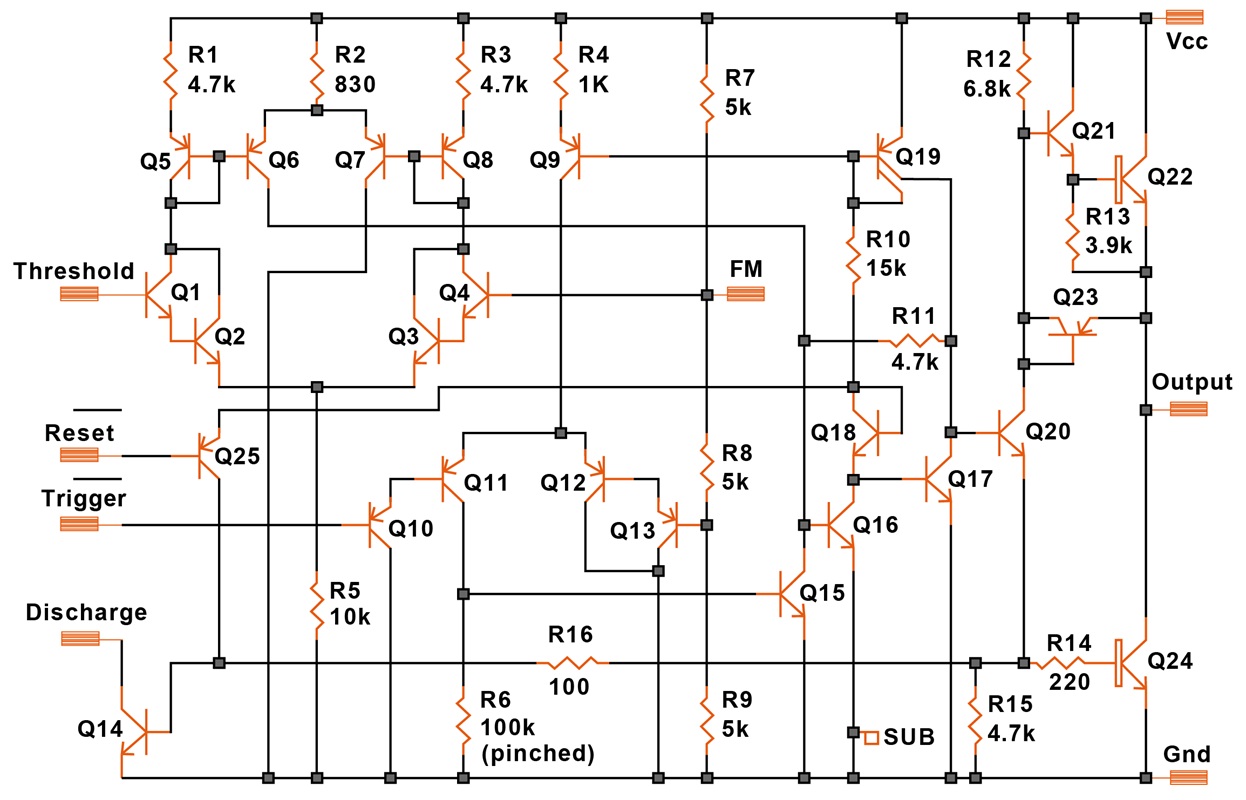
Figure 13-3. The original 555 timer. [click to enlarge]
Both comparators use Darlington input stages. This makes the timer fairly slow, but allows an extreme range of external resistance.
Comparator 1 consists of Q1 to Q8. The four PNP transistors (Q5 to Q8) form a current mirror with gain provided by the unequal emitter resistors. The output of this comparator feeds into a 4.7 kΩ resistor (R11), which is part of the cross-connection in the flip-flop (Q16, Q17). Comparator 2 (Q10 to Q15) resets the flip-flop.
The output stage, which must be able to sink or source some 200 mA, is controlled by Q20. In the logic-high output state, the Darlington pair Q21/Q22 delivers the current, but at the cost of about a 2 V drop.
In the logic-low output state, Q24 receives sufficient base current to work alone up to about 50 mA. Beyond that, as the voltage drop increases, Q23 feeds extra current into the base circuit.
Flaws of the Original 555 Timer
There are several flaws in this design, indicative of both the early period of IC design and the inexperience of a rookie designer. Neither comparator is well-balanced, with each having an offset of as much as 30 mV. The circuit can get away with that because the voltage swing is quite large.
The operating currents are also quite large—the lateral PNP transistors run at up to 1 mA. That was acceptable at the time, since the devices had 10 μm geometries. Today, however, it would be excessive.
The output stage consumes a considerable amount of current in the low state. Also, during switching, both output transistors are on for a brief period of time, producing a current spike in the supply.
Now, let’s examine the operation of the 555 timer in a few different configurations.
Operation of the 555 as a Timer
Figure 13-4 shows the 555 circuit configured as a timer.
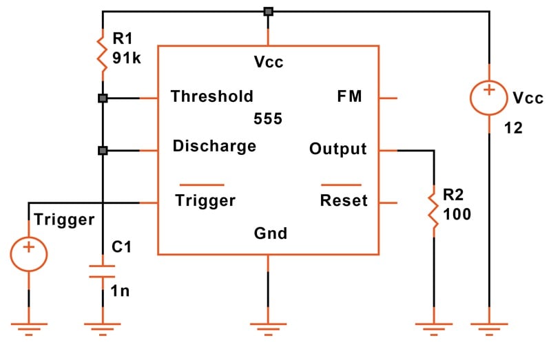
Figure 13-4. Timer connection of the 555.
In the timer configuration, the period starts with a negative-going trigger pulse, which resets the flip-flop through Comparator 2 and moves the output high. When the voltage across C1 reaches 2/3 Vcc, Comparator 1 sets the flip-flop, C1 is rapidly discharged, and the output moves low.
Despite the bad offset voltage, the accuracy is quite remarkable: the error in timing is around 1% with a temperature coefficient of 24 ppm/°C. The timing formula is:
$$t~=~1.1 ~\times~ R_1 C_1$$
Figure 13-5 shows the resulting waveforms.
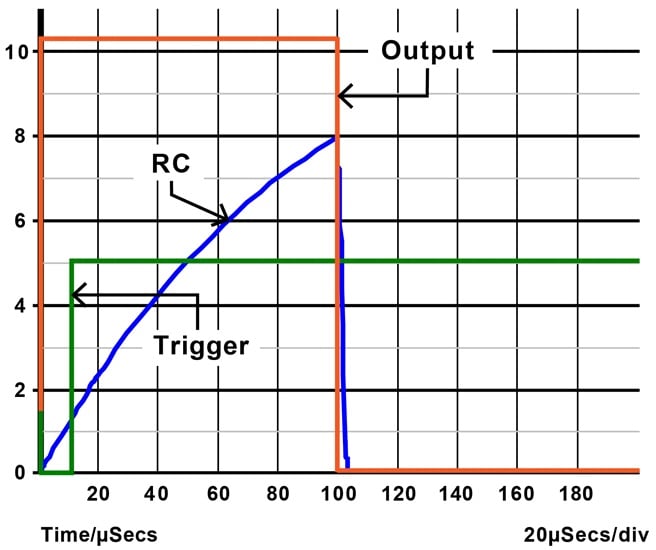
Figure 13-5. 555 timer waveforms.
Operation of the 555 as an Oscillator
Next, let’s look at the oscillator connection (Figure 13-6).
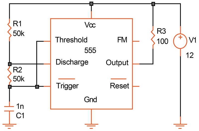
Figure 13-6. Oscillator connection of the 555.
There are two external resistors in the oscillator connection. The voltage across C1 moves between 1/3 Vcc and 2/3 Vcc with a frequency of:
$$f ~=~ \frac {1.46}{(R_1 ~+~ 2R_2) C_1}$$
and a duty cycle of:
$$\text{Duty cycle} ~=~ \frac {R_2}{R_1 ~+~ 2R_2}$$
The oscillator waveforms are illustrated in Figure 13-7.
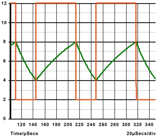
Figure 13-7. Oscillator waveforms.
An Updated 555 Design
The flaws in the original 555 design are:
- It’s not quite possible to achieve a 50% duty cycle.
- Charging and discharging the timing capacitor through a resistor connected to the output isn’t such a good idea.
- The high and low voltage drops are unequal and have significant temperature coefficients.
A CMOS version of the 555 exists. There’s also a redesign that can operate from a single battery cell (Redesigning the old 555). However, the circuit is still being sold today in its original form, despite the fact that much better performance is possible with more modern design techniques. Figure 13-8 is my candidate.
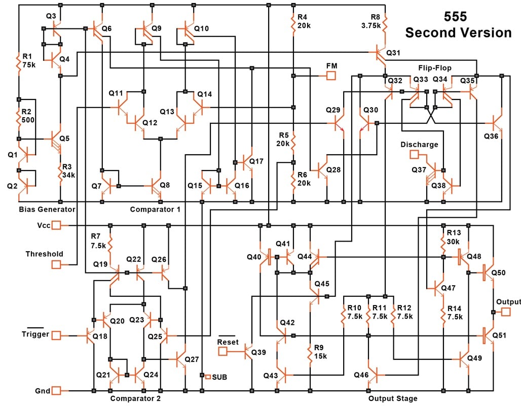
Figure 13-8. An improved version of the 555 timer, 33 years after the original design. [click to enlarge]
First off, the new timer gets a proper bias circuit (Q1 to Q5) to hold the operating currents more constant over the wide supply voltage range. This, together with a few other steps, extends the operating voltage down to 3 V.
Comparator 1 (Q6 to Q17) now has a balanced active load (Q15, Q16), which reduces the error in the timer mode to about 0.5% and the temperature drift to 3 ppm/°C without any loss in speed. The change in timing from 3 to 15 V is a mere 0.05%.
There are two changes in Comparator 2 (Q18 to Q27):
- A small operating current for the outer Darlington transistors. This greatly improves switching speed.
- A balanced active load. This makes the trigger level considerably more accurate.
The flip-flop (Q28 to Q36) is a new design. It operates in current-mode for maximum speed at the lowest possible current.
The two 50 μA currents generated by Q31 are split by a pair of lateral PNP transistors. One quarter of the current is fed into the base of the opposite flip-flop transistor, another quarter turns the reset transistor ON and OFF, and the remaining one half of the current steers the output stage. The voltage swing at the collectors of the flip-flop transistors (Q30, Q36) is 2VBE.
The Output Stage of the Improved 555 Timer
The most significant change is in the output stage. The base current for the lower output transistor (Q51) is no longer derived from a resistor. A small amount of current is injected into the bases of three transistors. These currents are forced to be equal by the three resistors R10, R11, and R12.
This, plus an additional current delivered by Q45, starts a positive feedback loop. The loop is formed by Q40, Q41, and Q42. This loop then provides whatever current is needed to keep Q51 fully turned on. Q40 is about seven times the size of Q41. Q42 has one emitter, while the output transistor has 24.
Positive feedback loops are always dangerous, as they can run away or refuse to turn off. In this case, the loop is contained by the collector resistance of Q43 and can be opened up by turning Q43 off.
Replacing the Darlington configuration in the upper part of the output stage with a compound (PNP/NPN) transistor reduces the voltage drop. The base current for this part is provided by Q47. Q44, Q46, and Q49 aid in turning the power devices off rapidly. They also eliminate the large transient current.
With these measures in place, the circuit’s typical current consumption is now reduced from 3 mA to 0.85 mA at 5 V. At 15 V, the new circuit consumes 1.2 mA. That’s down from 10 mA in the original version. The minimum operating voltage is 2.5 V from –40 to 100 °C.
CMOS 555 Timers
Shortly after the 555 came out, Intersil announced a CMOS version. It was (and still is) done in a 15 V process, which requires large dimensions and is inherently slow. The circuit isn’t directly compatible with the bipolar version, lacking high current outputs.
Except for these weaknesses, CMOS is ideally suited for a timer. There’s no input current and thus no need for Darlington stages.
Figure 13-9 shows a CMOS 555 design that uses a more modern 5 V (0.5 μm) process.
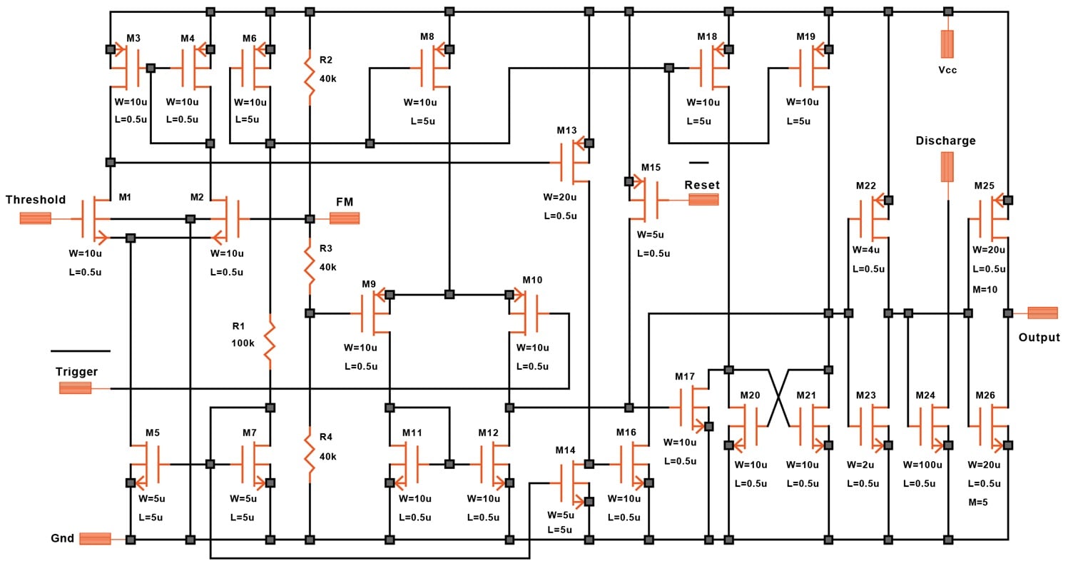
Figure 13-9. A 5 V CMOS version of the 555 timer. [click to enlarge]
The comparators are conventional. The dimensions of the devices are chosen so that the threshold and trigger inputs can move rail to rail. Their matching is adequate for precision operation (3 ppm/°C).
Ordinarily, a flip-flop consists of two cross-coupled gates. In this case, two cross-connected transistors fed by current sources result in smaller temperature and voltage drifts, because the flip-flop switch levels track the operating currents of the comparators.
The operating currents are set by R1, which limits the operating voltage range for high precision from 3 to 5 V. Replacing R1 with a current source extends this range down to 1 V.
A CMOS output stage swings rail-to-rail. The timing resistor can therefore be connected to the output as in Figure 13-10 to generate a square wave with a precise 50% duty cycle. By contrast, a bipolar output has a minimum drop of some 150 mV at the very least, if not an entire VBE.
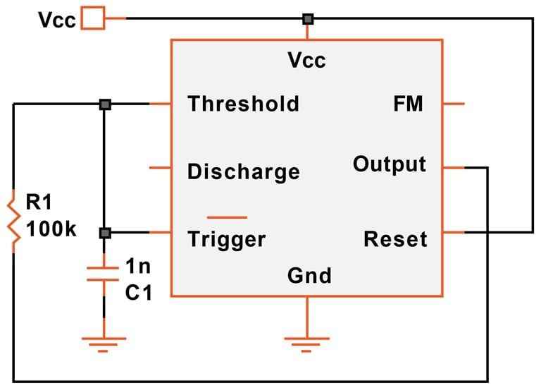
Figure 13-10. 50% duty cycle oscillator using a CMOS 555 timer.
On the other hand, CMOS devices are inferior to bipolar ones when it comes to current handling. Even with gate widths of 200 μm for the P-channel devices and 100 μm for the N-channel transistor, the circuit only delivers 10 mA. Furthermore, the voltage drop is 0.25 V, which badly affects the duty cycle. It would be better to have separate outputs for the timing resistor and the load.


