Facebook
 Google
 GitHub
 Linkedin
Crystal Oscillators
Let's start our discussion of crystal oscillators with the commonly-used CMOS circuit illustrated in Figure 13-23.
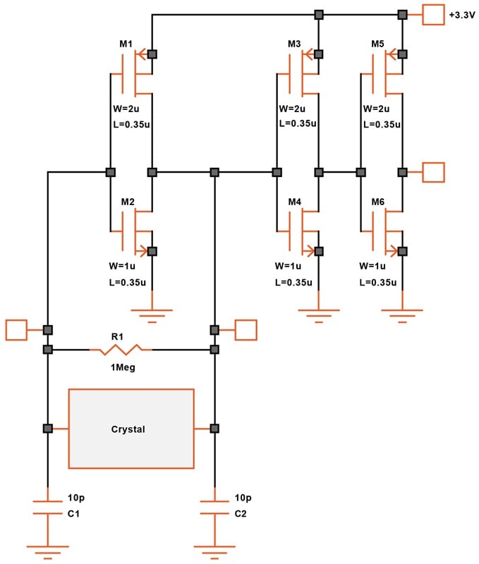
Figure 13-23. CMOS crystal oscillator. [click to enlarge]
The crystal is connected between the input and the output of an inverter. Since an inverter is ill-equipped to remain in a state between low and high, R1 is employed to force it—at least initially—into the linear region.
C1 and C2 are a mystery to most designers. They’re there because the crystal manufacturer specifies them.
The whole arrangement is a bit curious. An oscillator needs to have positive feedback, yet the phase-shift between the input and the output of an inverter is 180 degrees—negative feedback. To understand this, we need to look at the crystal itself.
Modeling the Crystal
Quartz is piezoelectric: a voltage applied across the quartz surfaces makes it flex, which creates a voltage between its surfaces. For circuit timing applications, a crystal is simply a sliver of quartz that vibrates.
The vibrating mass of the crystal can be represented as a series-resonant LC circuit (C1, L1) with a series resistance of R1. This is illustrated in Figure 13-24. C2 is the stray capacitance created by the contacts to the crystal and the wires and pins of the package.
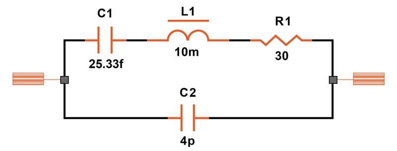
Figure 13-24. Model of a crystal.
The quality factor (Q) of such an LC circuit is given by:
$$Q ~=~ \frac {2 \pi f L_1}{R_1}$$
and its resonant frequency (f) by:
$$f ~=~ \frac {1}{2 \pi \sqrt {L_1C_1}}$$
Note that the values in Figure 13-24 were chosen to give a series-resonant frequency of exactly 10 MHz and a Q-factor of 20,000. Crystals have Q-factors in the range of 10,000 to 2 million—far higher than those of LC circuits. Ceramic resonators, which are otherwise almost identical to crystals, also have considerably lower Q-factors.
If we open the feedback loop in Figure 13-23, we can see what’s happening: there are, in fact, two resonances, about 0.2% apart from one another. The lower one is the series resonance; the higher one is the parallel resonance. As Figure 13-25 shows, the phase shifts abruptly between 180 and 0 degrees at these two frequencies.
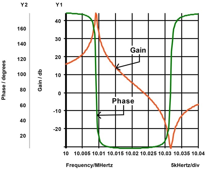
Figure 13-25. Series and parallel resonance of a crystal.
Improved CMOS Crystal Oscillator
The parallel resonance is created by C1, C2, and the combination of external capacitances. In an oscillator properly designed for series resonance, such as the one shown in Figure 13-26, the parallel resonance is of no concern.
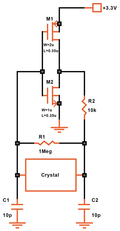
Figure 13-26. Improved CMOS crystal oscillator. [click to enlarge]
However, even the series resonance is influenced by the additional capacitances. As you might notice from the plot of Figure 13-25, the series resonance frequency is not exactly 10 MHz. There are two reasons for this:
- At resonance the phase moves from 180 degrees to zero, but it doesn't actually reach zero (the condition required for oscillation) until about 10.015 MHz.
- At resonance, the impedance of a series resonant LC circuit becomes very low, limited only by R1. It therefore works best if the input impedance of the inverter is low.
In Figure 13-23, all we have for input impedance is a 10 pF capacitance plus the gate capacitances. Thus, C1 of the crystal sees itself in series with this 10 pF capacitance, making the effective capacitance slightly smaller.
In the circuit of Figure 13-26, we shift the phase in the feedback loop with an additional resistor (R2) working against C2. Now, we reach a zero degree phase-shift at the series-resonant frequency. This is illustrated in Figure 13-27.
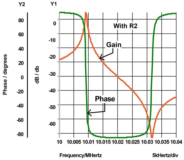
Figure 13-27. The insertion of R2 in Figure 13-26 brings the phase shift to zero degrees at the series resonance.
With R2, the frequency is more accurate. The chances of the crystal operating at some unwanted frequency (including harmonics) are diminished. However, be aware that R2 decreases the loop gain—make sure it safely exceeds unity.
The Challenge of Simulation
Simulating a crystal oscillator can be a frustrating task. The higher the Q-factor, the longer it takes for the oscillation to build up. For the circuit of Figure 13-26, it takes 3 ms for the oscillation to reach full amplitude as shown in Figure 13-28. That means you have to wait for 30,000 cycles before you can see the actual waveform.
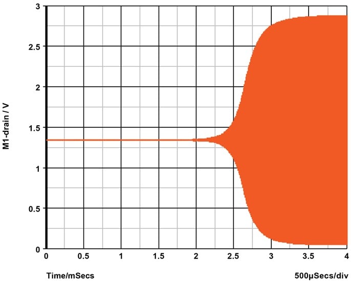
Figure 13-28. Start-up of a crystal oscillator.
If you want to measure the frequency accurately, you need to simulate using very fine time steps (say, 1 ns). Therefore, our 3 ms simulation will require 3 million time steps.
Bipolar Crystal Oscillator
Figure 13-29 shows a crystal oscillator circuit design using a bipolar process.
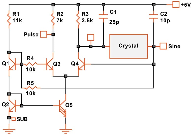
Figure 13-29. Alternate crystal oscillator with bipolar devices.
Here, the gain and a 180 degree phase-shift are obtained through Q4, which needs to run at a fairly substantial current (about 1 mA for the differential pair). The base of Q4 is biased at 2VBE, which gives sufficient voltage swing without saturating the transistor.
Q3, on the other hand, saturates. By making its collector-resistor larger than that of Q4, we obtain a pulse (square-wave) output that swings between 0.5 and 5 V.