Facebook
 Google
 GitHub
 Linkedin
CMOS Transconductance Amplifiers
The concept of the transconductance amplifier works in CMOS, too. However, the fundamentals are different. A CMOS transistor naturally takes a voltage at the gate and delivers a current at the drain, and this transconductance varies as the square of the operating current.
Figure 12-5 is the same configuration as shown in Figure 12-1, but with NPN transistors replaced by N-channel devices and PNP transistors by P-channel ones.
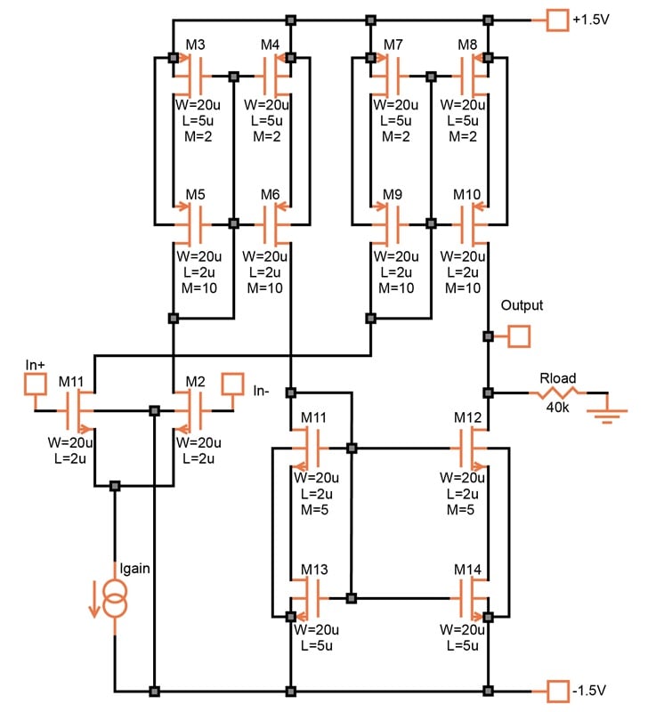
Figure 12-5. A CMOS transconductance amplifier. [click to enlarge]
The devices in this circuit are quite large: M5, for example, has a total width of 200 μm with the multiplier (M) set at 10. And yet, as we will discover shortly, the sizes chosen are still marginal.
In our CMOS transconductance circuit examples, we are using a dual power supply of ± 1.5 V. This may be an impractical value for you, but it was chosen to simplify the discussion of input and output DC levels. In the real world, you may be forced to use a single 3.0 or 3.3 V supply, in which case the inputs and the output have to be biased at half the supply voltage.
This circuit uses a 0.35 μm process. This is necessary because the high-accuracy current mirrors can’t tolerate an output voltage of less than about 0.6 V across them. If you were to use a process with smaller dimensions, you would have to reduce each mirror from four to two devices and pay the penalty of much-reduced accuracy.
Gain and Nonlinearity
A CMOS transconductance amplifier suffers from the same nonlinearity as a bipolar one. Distortion is tolerable only for small input signals. With a ± 40 mVpeak input, distortion is:
- 0.1% at 100 μA.
- 0.7% at 10 μA.
- 1.4% at 1 μA.
When the signal is increased to ± 75 mVpeak (which results in the maximum output swing possible, ± 0.9 V), the distortion increases to:
- 0.8% at 100 μA.
- 2.3% at 10 μA.
- 4.5% at 1 μA.
Figure 12-6 plots the gain versus the operating current for this circuit.
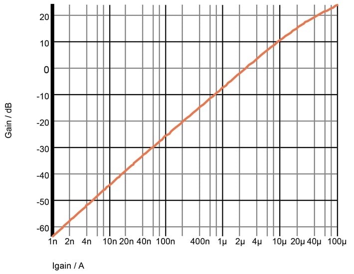
Figure 12-6. Gain (in dB) vs. Igain for the CMOS transconductance amplifier.
In this plot, the range is extended down to 1 nA just to show the wide range that’s achievable. Notice, however, that the circuit deviates from pure logarithmic behavior at the high end. To straighten this line, the transistors would have to be even larger.
Linearizing the Input of the CMOS Transconductance Amplifier
The transconductance of an MOS transistor is temperature-dependent. Because of this, the gain (at any current) decreases by about 2 dB from 0 to 100 °C. CMOS transconductance amplifiers also have the same offset problem as bipolar ones. At 100 μA, the offset is about ± 30 mV. Unlike its bipolar counterpart, the CMOS circuit in Figure 12-5 has no DC input current.
A rather complex scheme has been developed to linearize the input stage and still have gain control (see Design of Linear CMOS Transconductance Elements). As illustrated in Figure 12-7, it requires 15 more transistors (M15 to M29).
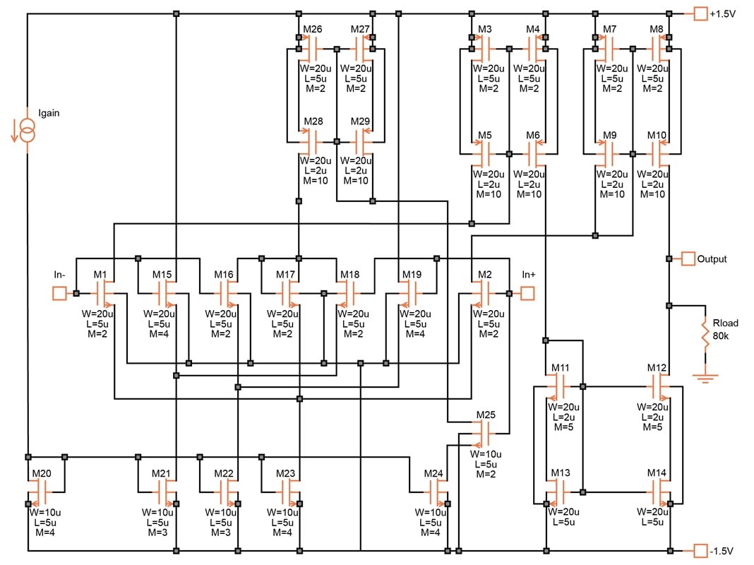
Figure 12-7. Transconductance amplifier with linearized input. [click to enlarge]
M17 is the key device. This diode-connected transistor is the same size as M1 and M2, the input differential pair. All three devices—M1, M2, and M17—share a mirrored Igain current (M23) at their sources.
The drain/base node of M17 receives the same amount of current from M24 through the current mirror created by M26 to M29. M25, a cascode transistor, has been added to improve the matching of the mirrored currents.
The current into the drain/base node of M17 is also shared by M16 and M18. However, their current is governed by the fact that they each are part of another differential pair (M16/M19 and M18/M15, respectively) whose operating currents are set at (3/4)Igain. M15 and M19 are twice as wide as the other five devices in the input row.
This complicated use of ratios serves to extend the input voltage range over which the differential pair is linear. The optimum input voltage range exceeds ± 1 V using a ratio of 2.155 between M15/M18 and M19/M16.
In the case we’re examining, this is of little consequence. 75 mV causes an output swing of ± 0.9 V, the maximum the circuit can handle. At this level, the distortion is:
- 0.1% at 50 μA.
- 0.2% at 5 μA.
- 0.3% at 0.5 μA.
Figure 12-8 plots the gain for this circuit.

Figure 12-8. Gain (in dB) vs. operating current (Igain) for the linearized CMOS transconductance amplifier.
With the device dimensions shown in Figure 12-7, the circuit can’t handle much more than 50 μA for Igain. It starts deviating slightly from the ideal logarithmic line above 20 μA. Due to the many additional devices, there’s also a slight deviation below about 10 nA. Even so, the gain control has a range of more than 70 dB.
Note that the output impedance is rather high. A buffer may be needed.
The problem with the offset voltage is still present, being only slightly reduced by the lower gain. You should figure on a ± 20 mV uncertainty at the output. For this reason, transconductance amplifiers are primarily used in audio and filter applications where the output can be capacitively coupled.