Facebook
 Google
 GitHub
 Linkedin
Bipolar Transconductance Amplifiers
For a while, it looked like there would be a second universal building block. The concept was called the operational transconductance amplifier, or OTA for short. However, the OTA has rather severe limitations. There’s no danger that it might dethrone the op amp anytime soon.
Let's examine the concept using the simple bipolar design in Figure 12-1.
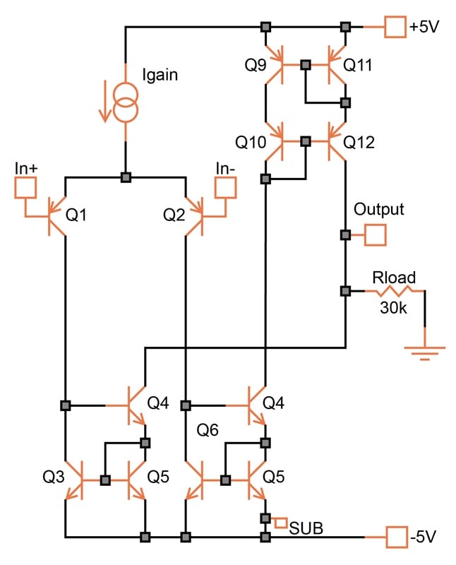
Figure 12-1. A simple bipolar transconductance amplifier. [click to enlarge]
Just as in an op amp, there’s a differential input pair (Q1, Q2). Its collector currents are mirrored separately by Q3–Q5 and Q6–Q8. One of the mirrored currents goes directly to the output through Q4. The second current is mirrored again (by Q9–Q12) and then opposes the first one at the output.
No matter what value is chosen for the operating current (Igain), the two currents at the output have the same value, and the output voltage is at ground. These conditions are at least true without an input signal (In+ = In–).
The Dynamic Emitter Resistance
Ignore Rload for a minute. As we saw in the Introduction to Differential Pairs, a bipolar transistor has an emitter resistance of:
$$r_e ~=~ \frac {kT}{I_eq}$$
where:
k and q are constants
T is the temperature in Kelvin
Ie is the emitter current.
The term for re is dynamic emitter resistance (often called "little re") because it changes with emitter current. At Ie = 1 mA, re is roughly 26 Ω (at room temperature). At 100 μA, it is 260 Ω, and at 10 μA, it is 2.6 kΩ. In short, it’s inversely proportional to Ie.
In series with the dynamic re, there’s also a constant resistance: the physical resistance between the emitter contact and the base-emitter junction. This becomes significant at higher currents.
BJT Transconductance
The transconductance of a bipolar transistor is simply:
$$g_m ~=~ \frac {1}{r_e}$$
With an emitter current of 100 μA, the transconductance is therefore:
$$g_m ~=~ \frac {1}{r_e} = \frac {1}{260} = 3.85 \text{ mS}$$
In other words, a 1 mV signal at the base causes a 3.85 μA change in collector current. In a differential stage, the transconductance is half of that since there is an re in each transistor. We must double the total current (Igain = 200 μA) so that each emitter receives 100 μA.
In Figure 12-1, the currents are mirrored with a ratio of 1:1 so that the collector currents of Q1 and Q2 appear unchanged at the output. With no signal at the input, they cancel each other. However, as one input is moved up or down, one current becomes larger and the other one smaller by the same amount. Thus, the total transconductance is doubled, and we have the same value as for a single transistor.
The Importance of Load Resistance
Without some DC resistance at the output, a transconductance amplifier is really quite impractical. Even the slightest mismatch in any of the transistors would slam the output voltage into one of the supply rails. We therefore need to add some impedance, Rload, to keep this voltage near the center.
Rload converts the current output into a voltage output, which means that we no longer have a transconductance amplifier. Instead, the circuit is simply a voltage amplifier—with a high output impedance to boot. Very few OTAs are actually used as transconductance amplifiers.
With Rload back in the circuit, the total voltage gain is now simply:
$$A_v ~=~ \frac {R_{load}}{r_e} ~=~ \bigg( \frac {q}{kT} \bigg) ~\times~ I_e ~\times~ R_{load}$$
From this equation, we see that the amplifier’s gain can be varied over a wide range by varying the current.Therein lies the problem. The input signal also varies the current, and so the gain changes with the amplitude of the signal. The result: distortion.
With a small signal at the input, this may be tolerable for some applications. With a large signal, it’s not. The following tables provide an overview of the gain and distortion:
Table 12-1. Gain as a function of current for transconductance amplifiers.
| Igain | 1 μA | 10 μA | 100 μA |
| Gain | –5 dB | 14 dB | 32 dB |
Table 12-2. Distortion as a function of current and input signal for transconductance amplifiers.
| Igain | 1 μA | 10 μA | 100 μA |
| Input Signal | Distortion | ||
| 10 mVpeak | 0.3% | 0.2% | 0.1% |
| 20 mVpeak | 1.2% | 0.9% | 0.3% |
| 50 mVpeak | 6.2% | 5.1% | 1.6% |
| 100 mVpeak | 16% | 15% | 8.0% |
Basically, if you have to handle a signal greater than about 20 mVpeak, this circuit is a poor choice. You can’t use feedback or emitter resistors for Q1 and Q2 to linearize it—it would interfere with the variable gain.
Dealing With Offset
Another problem—not just for this circuit, but for all such schemes—is offset. Mismatch in the input stage and any of the three current mirrors will show up as an offset, plus added distortion, at the output.
As Igain increases, the magnitude of this offset increases as well. In the circuit above operating at 100 μA, the worst-case offset is 60 mV. Also, remember that bipolar transistors have input currents.
There is help, though, as Figure 12-2 illustrates. As usual, you need to add a few more devices. If we connect diodes (Q16 and Q17) to the inputs and feed the signal in through resistor R1, we have something very similar to a current mirror.
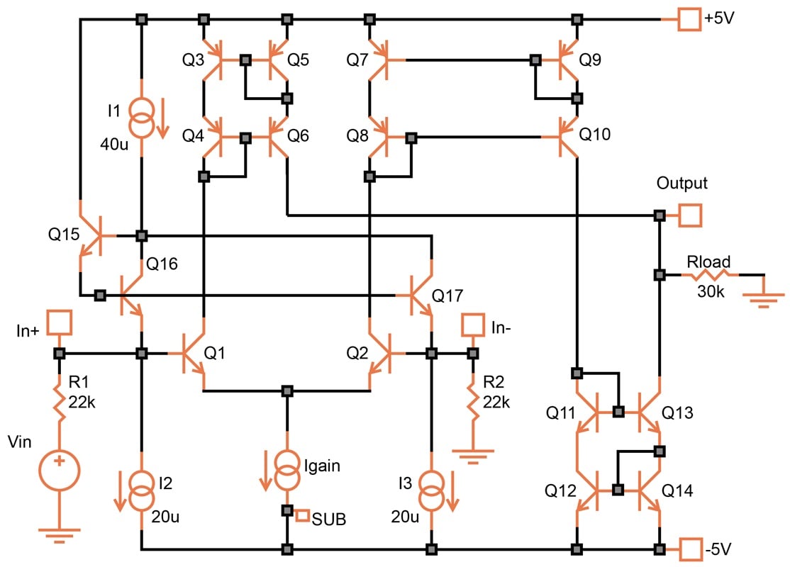
Figure 12-2. An improved version of the bipolar transconductance amplifier with linearizing diodes. [click to enlarge]
The input impedance is low because of Q16—at 20 μA, re is 1.3 kΩ at room temperature. R1 converts the input voltage into a current.
A 500 mVpeak input signal causes so little change in the voltage at the base of Q1 that the distortion is down to 0.3% at 1 μA and 0.01% at 100 μA. The offset voltage still persists, again 60 mV worst-case at 100 μA.
To avoid worse offset problems, both sides of the input pair need to be treated equally. This includes the addition of the dummy resistor R2. The current mirrors used here are of the highest precision, sacrificing low operating voltage for accuracy.
Q15 aids in removing the base currents for Q16 and Q17 from I1. Even with the addition of Q15, the ratio between I1 and I2/I3 needs to be precise. Any mismatch will increase the offset voltage and the input current (250 nA max with perfect matching).
Gain Control
The one great feature of a circuit like this is the precise control of gain over a wide range. Figure 12-3 shows the gain (in dB) vs. Igain.
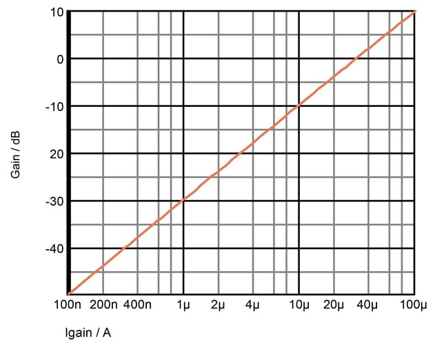
Figure 12-3. Gain is a precise logarithmic function of Igain.
A linear change in current results in a logarithmic change in gain. Thus, for audio applications, you can control the volume (a logarithmic function) with a linear current or voltage. The accuracy is within ± 0.2 dB. True to the exponential nature of the base-emitter diode, the gain changes 20 dB per decade of current.
Because the diode-connected transistors (Q16 and Q17) track the input transistors, gain is virtually unaffected by temperature. If Igain is derived from a resistor made from the same layer as R1, R2, and Rload, the gain is also unaffected by absolute variations. Figure 12-4 shows the output’s waveforms as a function of gain current for a 1 kHz sinusoidal input.
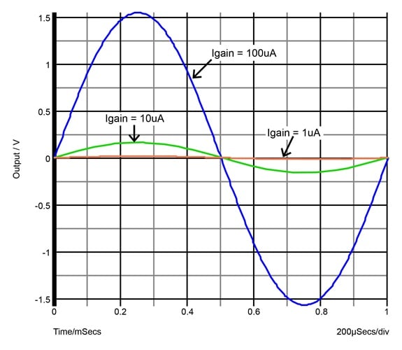
Figure 12-4. Output as a function of gain current for the improved bipolar transconductance amplifier.
In this figure, we see that there’s a very large change in the level of the signal. This is, of course, the purpose of the circuit. Because of the offset voltage, a transconductance amplifier is best suited for audio and filter applications with the output capacitively coupled to the next stage.