Facebook
 Google
 GitHub
 Linkedin
Slope (integrating) ADC
So far, we’ve only been able to escape the sheer volume of components in the flash converter by using a DAC as part of our ADC circuitry. However, this is not our only option. It is possible to avoid using a DAC if we substitute an analog ramping circuit and a digital counter with precise timing.
The is the basic idea behind the so-called single-slope, or integrating ADC. Instead of using a DAC with a ramped output, we use an op-amp circuit called an integrator to generate a sawtooth waveform which is then compared against the analog input by a comparator.
The time it takes for the sawtooth waveform to exceed the input signal voltage level is measured by means of a digital counter clocked with a precise-frequency square wave (usually from a crystal oscillator). The basic schematic diagram is shown here:
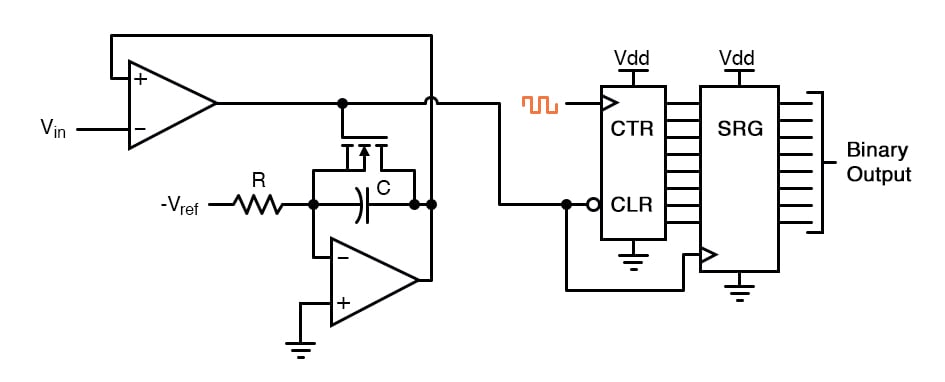
The IGFET capacitor-discharging transistor scheme shown here is a bit oversimplified. In reality, a latching circuit timed with the clock signal would most likely have to be connected to the IGFET gate to ensure full discharge of the capacitor when the comparator’s output goes high.
The basic idea, however, is evident in this diagram. When the comparator output is low (input voltage greater than integrator output), the integrator is allowed to charge the capacitor in a linear fashion. Meanwhile, the counter is counting up at a rate fixed by the precision clock frequency.
The time it takes for the capacitor to charge up to the same voltage level as the input depends on the input signal level and the combination of -Vref, R, and C. When the capacitor reaches that voltage level, the comparator output goes high, loading the counter’s output into the shift register for a final output.
The IGFET is triggered “on” by the comparator’s high output, discharging the capacitor back to zero volts. When the integrator output voltage falls to zero, the comparator output switches back to a low state, clearing the counter and enabling the integrator to ramp up voltage again.
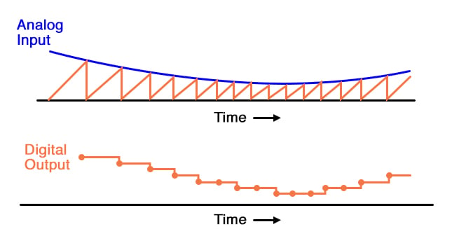
This ADC circuit behaves very much like the digital ramp ADC, except that the comparator reference voltage is a smooth sawtooth waveform rather than a “stairstep:”
The single-slope ADC suffers all the disadvantages of the digital ramp ADC, with the added drawback of calibration drift. The accurate correspondence of this ADC’s output with its input is dependent on the voltage slope of the integrator being matched to the counting rate of the counter (the clock frequency).
With the digital ramp ADC, the clock frequency had no effect on conversion accuracy, only on update time. In this circuit, since the rate of integration and the rate of count are independent of each other, variation between the two is inevitable as it ages, and will result in a loss of accuracy.
The only good thing to say about this circuit is that it avoids the use of a DAC, which reduces circuit complexity.
Dual-Slope Converter
An answer to this calibration drift dilemma is found in a design variation called the dual-slope converter. In the dual-slope converter, an integrator circuit is driven positive and negative in alternating cycles to ramp down and then up, rather than being reset to 0 volts at the end of every cycle.
In one direction of ramping, the integrator is driven by the positive analog input signal (producing a negative, variable rate of output voltage change, or output slope) for a fixed amount of time, as measured by a counter with a precision frequency clock. Then, in the other direction, with a fixed reference voltage (producing a fixed rate of output voltage change) with time measured by the same counter.
The counter stops counting when the integrator’s output reaches the same voltage as it was when it started the fixed-time portion of the cycle. The amount of time it takes for the integrator’s capacitor to discharge back to its original output voltage, as measured by the magnitude accrued by the counter, becomes the digital output of the ADC circuit.
The dual-slope method can be thought of analogously in terms of a rotary spring such as that used in a mechanical clock mechanism. Imagine we were building a mechanism to measure the rotary speed of a shaft.
Thus, shaft speed is our “input signal” to be measured by this device. The measurement cycle begins with the spring in a relaxed state.
The spring is then turned, or “wound up,” by the rotating shaft (input signal) for a fixed amount of time. This places the spring in a certain amount of tension proportional to the shaft speed: a greater shaft speed corresponds to a faster rate of winding and a greater amount of spring tension accumulated over that period of time.
After that, the spring is uncoupled from the shaft and allowed to unwind at a fixed rate, the time for it to unwind back to a relaxed state measured by a timer device. The amount of time it takes for the spring to unwind at that fixed rate will be directly proportional to the speed at which it was wound (input signal magnitude) during the fixed-time portion of the cycle.
This technique of analog-to-digital conversion escapes the calibration drift problem of the single-slope ADC because both the integrator’s integration coefficient (or “gain”) and the counter’s rate of speed are in effect during the entire “winding” and “unwinding” cycle portions. If the counter’s clock speed were to suddenly increase, this would shorten the fixed time period where the integrator “winds up” (resulting in a lesser voltage accumulated by the integrator), but it would also mean that it would count faster during the period of time when the integrator was allowed to “unwind” at a fixed rate.
The proportion that the counter is counting faster will be the same proportion as the integrator’s accumulated voltage is diminished from before the clock speed change. Thus, the clock speed error would cancel itself out and the digital output would be exactly what it should be.
Another important advantage of this method is that the input signal becomes averaged as it drives the integrator during the fixed-time portion of the cycle. Any changes in the analog signal during that period of time have a cumulative effect on the digital output at the end of that cycle.
Other ADC strategies merely “capture” the analog signal level at a single point in time every cycle. If the analog signal is “noisy” (contains significant levels of spurious voltage spikes/dips), one of the other ADC converter technologies may occasionally convert a spike or dip because it captures the signal repeatedly at a single point in time.
A dual-slope ADC, on the other hand, averages together all the spikes and dips within the integration period, thus providing an output with greater noise immunity. Dual-slope ADCs are used in applications demanding high accuracy.
RELATED WORKSHEET: