 Facebook
 Google
 GitHub
 Linkedin
Flash ADC
Also called the parallel A/D converter, this circuit is the simplest to understand. It is formed of a series of comparators, each one comparing the input signal to a unique reference voltage. The comparator outputs connect to the inputs of a priority encoder circuit, which then produces a binary output. The following illustration shows a 3-bit flash ADC circuit:
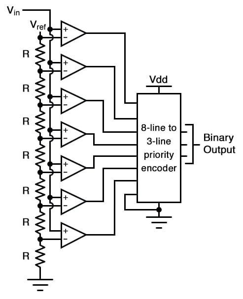
Vref is a stable reference voltage provided by a precision voltage regulator as part of the converter circuit, not shown in the schematic. As the analog input voltage exceeds the reference voltage at each comparator, the comparator outputs will sequentially saturate to a high state. The priority encoder generates a binary number based on the highest-order active input, ignoring all other active inputs.
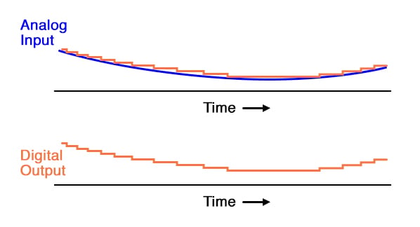
When operated, the flash ADC produces an output that looks something like this:
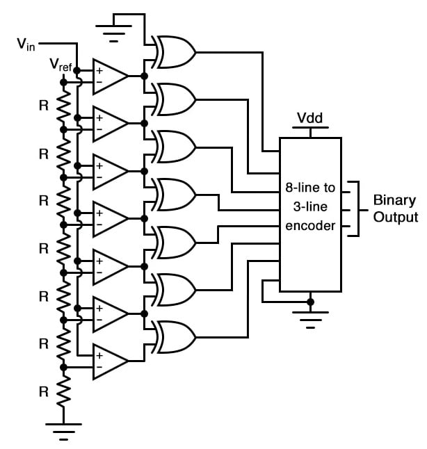
For this particular application, a regular priority encoder with all its inherent complexity isn’t necessary. Due to the nature of the sequential comparator output states (each comparator saturating “high” in sequence from lowest to highest), the same “highest-order-input selection” effect may be realized through a set of Exclusive-OR gates, allowing the use of a simpler, non-priority encoder:
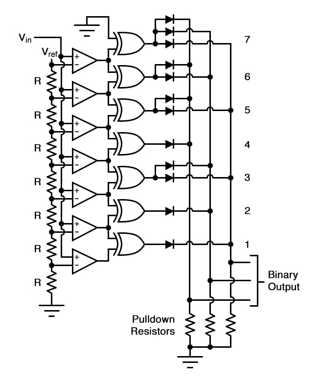
And, of course, the encoder circuit itself can be made from a matrix of diodes, demonstrating just how simply this converter design may be constructed:
Not only is the flash converter the simplest in terms of operational theory, but it is the most efficient of the ADC technologies in terms of speed, being limited only in comparator and gate propagation delays. Unfortunately, it is the most component-intensive for any given number of output bits.
This three-bit flash ADC requires seven comparators. A four-bit version would require 15 comparators. With each additional output bit, the number of required comparators doubles.
Considering that eight bits is generally considered the minimum necessary for any practical ADC (255 comparators needed!), the flash methodology quickly shows its weakness. An additional advantage of the flash converter, often overlooked, is the ability for it to produce a non-linear output.
With equal-value resistors in the reference voltage divider network, each successive binary count represents the same amount of analog signal increase, providing a proportional response. For special applications, however, the resistor values in the divider network may be made non-equal.
This gives the ADC a custom, nonlinear response to the analog input signal. No other ADC design is able to grant this signal-conditioning behavior with just a few component value changes.
RELATED WORKSHEET:


Thanks 😊 Helped me
Wonderful
What is the purpose of the top-most XOR gate in this design? In logic terms, it just repeats the input, so why not just connect the output of the top-most comparator straight through to the encoder?