 Facebook
 Google
 GitHub
 Linkedin
Introduction to the Operation of Bipolar Junction Transistor (BJT)
It is certainly possible to successfully implement bipolar junction transistors (BJTs) without thoroughly understanding their low-level electrical behavior. In fact, this is quite common, even among professional engineers, simply because the precise physical operation of semiconductor devices is a complex topic that is distinct from the equations and techniques that we use when incorporating semiconductor devices into a circuit.
Nevertheless, it’s important to have at least a general idea of what is occurring in an electrically active bipolar junction transistor, and this tutorial will provide that information.
Base, Emitter, Collector
Transistors are central components in electronic devices because they can function as amplifiers and switches—in other words, because they allow a small-amplitude input signal to modulate or control a large-amplitude output signal.
In a bipolar junction transistor, amplification results from the specialized interaction that occurs between an emitter region, a physically thin base region, and a wide collector region. We’ll use the structure of an npn transistor in this discussion; however, if you understand npn operation, you can understand pnp operation, because the same phenomena govern both types.
The following diagram will help you to visualize the physical operation of an npn transistor. However, be aware that this is not consistent with how integrated-circuit BJTs are actually fabricated.
![]()
The base-to-emitter junction acts like a typical pn junction. If we ground the emitter and apply sufficient voltage to the base, current will flow from base to emitter.
At this point the transistor is little more than a diode, but something interesting happens if we apply a voltage to the collector—more specifically, if we apply a voltage that is higher than the base voltage and therefore causes the base-to-collector pn junction to be reverse-biased.
Collecting Electrons
The base-to-emitter current consists of holes flowing from the p-type base to the n-type emitter and electrons flowing from the n-type emitter to the p-type base.
As mentioned above, the base region is thin, and now the collector has a positive voltage relative to the base; thus, most of those electrons will cross the base, reach the base-collector depletion region, and continue flowing into the collector region and out of the collector terminal.
![]()
Since the direction of conventional current is opposite to the physical flow of electrons, we now have current flowing from collector to emitter. Also, notice that the names of the terminals of an npn transistor make more sense if you think in terms of moving electrons rather than conventional current flow.
The emitter region emits (or injects) electrons, and the collector region collects the electrons that have diffused across the base region.
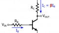
BJT Current Gain
At this point, current is flowing from base to emitter and from collector to emitter, but we still haven’t identified the true significance of BJT operation.
The critical detail here is that the collector-to-emitter current is much larger than the base-to-emitter current and determined by the base-to-emitter current. In other words, a small input signal applied to the base regulates a larger current flowing into the collector, and this is what we call amplification.
The mathematical relationship between the base current (IB) and the collector current (IC) is written as follows:
IC = βIB
The proportionality factor, written as the Greek letter β and often referred to as “beta” in spoken language, is the current gain exhibited by the BJT when it is operating in forward active mode—that is, when the base-to-emitter junction is forward-biased and the base-to-collector junction is reverse-biased.
Typical β values range from 50 to 200, and this reinforces the previous statement: a small base current results in a collector current that is dependent on and much larger than the base current.
![]()
Conclusion
The details of BJT current and voltage behavior go far beyond the information that we have covered in this video tutorial. Nonetheless, we’ve built a basic foundation for those who wish to focus on practical circuit design. In the next tutorial, we’ll discuss operating modes and plots that will help you to continue building your knowledge of BJT functionality and implementation.
Related Content


excellent explanation!