Facebook
 Google
 GitHub
 Linkedin
Current and Voltage Relationships in Bipolar Junction Transistors (BJTs)
The previous tutorial provided a low-level explanation of how a BJT functions when it is in the forward active mode. This is a good place to start, but you’ll need to know quite a bit more if your goal is to analyze or design BJT-based circuits. We’ll start with the three most common operational modes, and then we’ll look at some plots that will help us to understand the relationships between BJT currents and voltages.
Cutoff and Active Mode
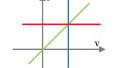
Let’s imagine that we’re working with the simple BJT circuit shown below.

If VIN is connected to ground, the base-to-emitter (BE) junction is not forward-biased. No significant amount of current flows into the base, and consequently no significant amount of current flows from collector to emitter. Thus, the transistor is in the nonfunctional mode called cutoff, and it will remain in this mode until the base voltage is high enough to forward-bias the BE junction.
When VIN is approximately 0.6 V, the BE junction begins to conduct. The base current IB, which is limited by the base resistor RB, determines the collector current: IC = βIB. The BJT is in forward active mode because the supply voltage connected to the collector through RC is much higher than VIN, and this ensures that the base-to-collector (BC) junction is reverse-biased.
It’s true that some voltage is dropped across the resistor RC, and consequently, the voltage at the collector is lower than 5 V, but we’ll assume that the collector resistance and the initial collector current are small enough to maintain conditions of reverse-bias for the BC junction.
Saturation Mode
As VIN increases, the base current increases and therefore so does the collector current. Eventually, the collector resistor RC will drop so much voltage that the BC junction will begin to enter the forward-bias region.
When both the BE junction and the BC junction are forward-biased, the transistor is in saturation mode. The BC junction enters the forward-bias region when the base-to-collector voltage is about 0.5 V; since the base-to-emitter voltage stays near 0.7 V and the emitter is grounded, a bit of math tells us that the voltage at the collector will be 0.2 V.
This is called the collector-to-emitter (VCE) saturation voltage: VCE(sat) = 0.2 V.

Current-Voltage Characteristics
In cutoff mode, the transistor is inactive; current cannot flow from collector to emitter. In forward active mode, increases in base current create increases in collector current according to the relationship IC = βIB. However, when the transistor enters saturation, the collector current essentially levels out: we can continue to raise VIN, but this will result in only very small increases in collector current.
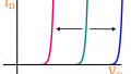
This behavior is shown in the following plot.

As you can see, VIN is increasing from 0 to 1.6 V. The collector current is extremely small until VIN reaches approximately 0.6 V. After that, the transistor is in forward active mode, and collector current increases rapidly.
Then, at VIN ≈ 1.05 V, the collector current reaches the point at which the voltage dropped across RC is large enough to move the BC junction into the forward-bias region. This is when the transistor enters saturation: though VIN (and consequently IB) continues to increase, the collector current is almost constant.
The next plot clarifies the relationship between collector current and forward bias of the BC junction.

VOUT, which is the same as the collector voltage, begins at 5 V and decreases as increasing collector current causes a progressively larger voltage drop across RC. As explained above, the BJT exits forward active mode when the base-to-collector voltage is 0.5 V, which corresponds to a collector voltage of 0.2 V.
This behavior is evident in the plot: collector current levels off when VOUT reaches approximately 0.2 V.
Conclusion
We’ve covered BJT operating modes, and now we’re ready to study some BJT applications. In the next tutorial, we’ll examine a circuit that uses a BJT as a high-current switch, and after that we’ll look at a BJT-based amplifier.