 Facebook
 Google
 GitHub
 Linkedin
Using Operational Amplifiers as Comparators
This article discusses the specifications and characteristics to consider when using op-amps as comparators and provides a design procedure.
This article discusses the specifications and characteristics to consider when using op-amps as comparators and provides a design procedure.
Comparators are often used to differentiate between two conditions in a system: For example, outputting a logic high (5V) in an overvoltage situation and a logic low (0V) for normal operation. Along with dedicated comparators, it’s possible to configure operational amplifiers (op-amps) to operate as comparators.
Op-amps have several benefits over dedicated comparators, costing less and minimizing printed circuit board (PCB) area. However, you must consider multiple op-amp specifications or characteristics before configuring an op-amp as a comparator.
Design Considerations
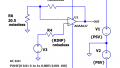
When configuring an op-amp as a comparator, you need to consider the presence of differential input clamping diodes (back-to-back diodes), the input common-mode voltage, the slew rate and the overload recovery time. Figure 1 shows a typical comparator configuration when using an op-amp.
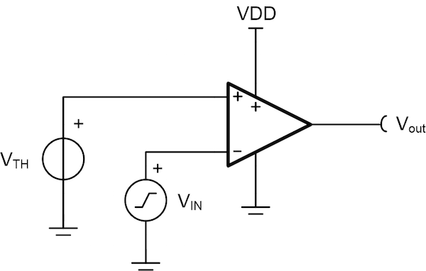
Figure 1. The typical comparator configuration using an op-amp.
Differential Input Clamping Diodes
Differential input clamping diodes, also called back-to-back input diodes, protect the input stage transistors from large differential input voltages. Figure 2 shows the internal differential input clamping diodes.
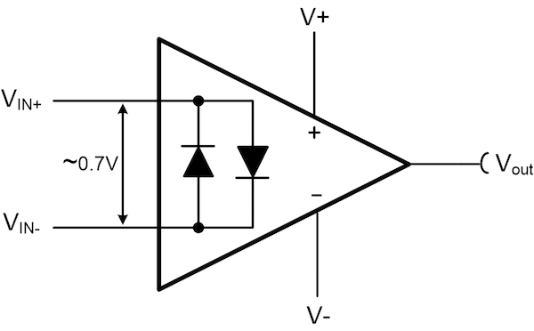
Figure 2. Input clamping diodes
An op-amp cannot have differential input clamping diodes when used as a comparator. When applying a differential signal larger than a diode drop to an op-amp with differential input clamping diodes, one of the diodes between the noninverting and inverting inputs will conduct, shorting the two inputs together. During this condition, excessive current will flow through the appropriate diode, potentially damaging the device. Figure 3 illustrates this effect when the input diode conducts and current flows from a reference source (VRef) to the input voltage (Vin).

Figure 3. The clamping diode conducts when the differential input is too large.
Input Common-Mode Voltage
The common-mode voltage range defines the linear operating region of an op-amp’s input stage. The voltage on the op-amp’s inputs should be within this range; otherwise, undesirable results such as phase inversion.
Propagation Delay
When configuring an op-amp as a comparator, the propagation delay is the total time for the output voltage to transition from low to high or high to low after the input transitions. The total transition time depends on the op-amp’s overload recovery time and slew rate. Equation 1 calculates the total op-amp output transition time:
tTOTAL = tOL + tS
where tOL is the overload recovery time and tS is the time to slew.
The input voltage should not change until the output settles to its final value. Figure 4 displays a typical output voltage waveform of an op-amp configured as a comparator. Notice that the output voltage completely transitions before the input changes.

Figure 4. Propagation delay
Overload Recovery Time
Overload recovery time is the time required for the output voltage to begin changing from a saturated condition after a change in input voltage. An op-amp’s overload recovery time will affect signal timing if the overload recovery time is too long for a high-frequency input signal because the output may not be able to reach the final amplitude level for a “high” or “low” state before the input signal changes again.
Figure 5 displays how overload recovery can affect timing when configuring an op-amp as a comparator. In this example, tOL causes tTOTAL to exceed the allowable transition time. The green dashed line displays correct timing when the overload recovery time is fast enough for the input signal frequency. The output waveform’s solid line indicates a situation where the device overload recovery time is too long. Notice that the output does not reach the final amplitude before the input signal changes, leading to potential timing errors, shown as ΔV in Figure 5.

Figure 5. Influence of overload recovery time to timing
Slew Rate
Slew rate is the maximum rate of change of an op-amp’s output voltage, thus affecting the rise and fall times of Figure 4’s output waveform. For comparator applications, the output usually needs to change from high to low or low to high once the input voltage crosses the threshold voltage. Slew rate is a key specification because it limits the rate at which the output voltage can change. A lower slew rate takes longer for the output to reach the final amplitude, which may lead to timing errors if the input signal changes before the output voltage can reach a high or low state.
Figure 6 shows how slew rate affects timing when configuring an op-amp as a comparator. In this example, tS causes tTOTAL to exceed the allowable transition time. The green dashed line displays correct timing when the slew rate is fast enough for the output to reach a high or low state before the input signal changes. The output waveform’s solid line indicates a situation where the device has too slow of a slew rate. Notice that the output does not reach the final amplitude before the input signal changes, leading to potential timing errors, shown as ΔV in Figure 6.

Figure 6. Influence of slew rate on timing
The propagation delay contains effects of the overload recovery time and slew rate, which are each affected by the differential signal amplitude applied to the input. Increasing the differential input voltage or overdrive voltage can reduce the propagation delay time. Figure 7 shows how different amplitudes of input overdrive voltage affect propagation delay on the TLV9062. Notice that the larger the input overdrive voltage, the faster the propagation delay. Overdrive voltages less than 100 mV will result in longer propagation delays because the overload recovery time increases and the slew rate decreases.

Figure 7. Input overdrive voltage vs. falling edge propagation delay
Design Procedure
It’s possible to simplify the procedure for designing an op-amp as a comparator into two design steps:
- Set the threshold voltage using a resistor divider or reference voltage.
- Select an op-amp that meets all of the design requirements discussed here.
Figure 8 shows the TLV9062 configured as an inverting comparator. This device does not have input clamping diodes (a requirement to operating an op-amp as a comparator), features rail-to-rail input and output, and has a slew rate of 6.5 V/µs and an overload recovery time of 200 ns.

Figure 8. Comparator application using the TLV9062
For an inverting comparator topology, connect the input signal, VIN, to the inverting pin of the op-amp and the threshold voltage, VTH, to the noninverting pin of the op-amp. In this configuration, the output of the op-amp transitions high to the positive supply (V+) when the input signal is less than the threshold voltage and transitions low to the negative supply (GND) when the input signal is greater than the threshold voltage.
A resistor divider, R1 and R2, and the supply voltage, V+, set the threshold voltage for the design. Equation 2 calculates the threshold voltage. Setting resistor R1 equal to R2 sets the threshold voltage to mid-supply.

Application Curves
Using a 0- to 5-V triangle waveform for the input signal validates the comparator’s operation. A triangle wave input helps easily determine where the output transitions from high to low or low to high because the waveform is a slow-moving ramping input signal. Figure 9 displays the input signal (black) and output signal (red) waveforms. Notice that the output transitions after the input signal crosses the 2.5V threshold voltage.

Figure 9. Comparator response to input voltage (propagation delay included)
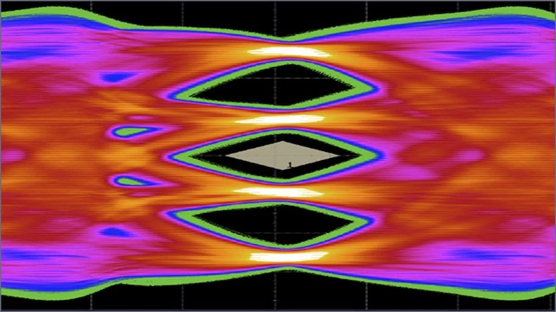
Figure 10’s zoomed-in screenshots of the rising and falling edges of Figure 9’s output signal show the effects that slew rate can have on circuit timing. The TLV9062 takes approximately 1 µs to transition from low to high (or high to low) because of the device’s slew rate.
.jpg)
Figure 10. Rising edge (left) and falling edge (right)
Conclusion
Op-amps configured to operate as comparators provide a low-cost and small PCB footprint alternative to dedicated comparators. You must consider four main op-amp characteristics to ensure expected performance, however:
- The input differential clamping diodes.
- The input common-mode voltage.
- The slew rate.
- The overload recovery time.
The op-amp must be void of input clamping diodes; otherwise, excessive current may flow through the inputs and cause damage. Do not exceed the input common-mode voltage range, or else undesirable effects such as phase reversal may occur. Finally, account for both slew rate and overload recovery in the output signal’s transition time to avoid timing errors and inaccurate readings in the circuit. By understanding how each of these characteristics affects circuit performance, you can design a robust and accurate system.
References
-
TI Precision Labs – Op-Amps Training
-
Trump, Bruce. “Op-amps used as comparators – is it okay?” TI E2E™ Community technical article, March 14, 2012.
Related Content


Your precaution against protection diodes is rather confusing given that I can easily find numerous examples on the internet (and I’ve also seen it done in commercial circuits) where external differential diodes are ADDED to op amp comparator circuits. I think it might be better to recommend including some resistors in series with the inputs to limit current through the diodes rather than admonish against using them at all…0.7V difference is plenty enough to send an open-loop op amp to its rails!