Facebook
 Google
 GitHub
 Linkedin
Using Zero-IF to Reduce PCB Footprint and Cost
Learn how to make more efficient designs for RF applications using Zero-IF architecture.
Learn how to make more efficient designs for RF applications using Zero-IF architecture.
Introduction
Zero-IF (ZIF) architecture has been around since the early days of radio. Today the ZIF architecture can be found in nearly all consumer radios, whether television, cell phones, or Bluetooth® technology. The key reason for this wide adoption is that it has proven time and again to offer the lowest cost, lowest power, and the smallest footprint solution in any radio technology. Historically, this architecture has been withheld from applications that demand high performance. However, with the demand for wireless growing around us and the rapidly crowding spectrums, a change is required in order to continue economically deploying radios in the infrastructure that supports our wireless needs. Contemporary zero-IF architectures can satisfy these needs as many of the impairments normally associated with these architectures have been resolved through a combination of process, design, partitioning, and algorithms. New advances in ZIF technology challenge the current high performance radio architectures and introduce new products with breakthrough performance to enable new applications previously beyond the reach of ZIF. This article will explore the many benefits of ZIF architectures and introduce new levels of performance that they bring to radio designs.
Challenges of the Radio Engineer
Today's transceiver architect is challenged by a growing list of demands driven by our ever increasing requirements for wireless devices and applications. This leads to the continual need to access more bandwidth.
The designer has moved over the years from a single carrier radio to multicarrier. As spectrum becomes fully occupied in one band, new bands are allocated; now there are more than 40 wireless bands that must be served. Because operators have spectrum in multiple bands and these resources must be coordinated, the trend is toward carrier aggregation, and carrier aggregation leads to multiband radios. This all leads to more radios, with higher performance, requiring better out-of-band rejection, improved emissions, and less power dissipation.
While the demand for wireless is rapidly increasing, the power and space budgets are not. In fact, with an ever increasing need to economize both in power and space, reducing both the carbon footprint and the physical footprint are very important. To achieve these goals, a new perspective on radio architectures and partitioning is required.
Integration
In order to increase the number of radios in a particular design, the footprints must be made smaller for each radio. The traditional way to do this is to progressively integrate more and more of the design onto a single piece of silicon. While this may make sense from a digital perspective, integration of analog functionality for the sake of integration doesn't always make sense. One reason is that many analog functions in a radio cannot effectively be integrated. For example, a traditional IF sampling receiver is shown in Figure 1. There are four basic stages to an IF sampling architecture: low noise gain and RF selectivity, frequency translation, IF gain and selectivity, and detection. For selectivity, SAW filters are typically used. These devices cannot be integrated and therefore must be off chip. While RF selectivity is provided by piezoelectric or mechanical devices, occasionally LC filters are used for the IF filter. While LC filters may occasionally be integrated on monolithic structures, the compromise in both filter performance (Q and insertion loss) and the required increase in sample rate of the digitizer (detector) increase the overall dissipation.
Digitizers (analog-to-digital converters) must be done on low cost CMOS processes to keep the cost and power reasonable. While they certainly can be fabricated on bipolar processes, this results in both larger and more power hungry devices, which runs counter to optimization for size. Thus standard CMOS is the desired process for this function. This becomes a challenge for integration of high performance amplifiers, particularly the IF stage. While amplifiers can be integrated on CMOS processes, it is difficult to get the performance required from processes that are optimized for low power and low voltage. Furthermore, integrating the mixer and IF amplifier on chip requires that the interstage signals be routed off chip to access the IF and antialias filters prior to being digitized, foregoing much of the benefit of integration. Doing so is counterproductive to integration as it increases the pin count and package size. Additionally, each time critical analog signals pass through a package pin, a compromise in performance is made.
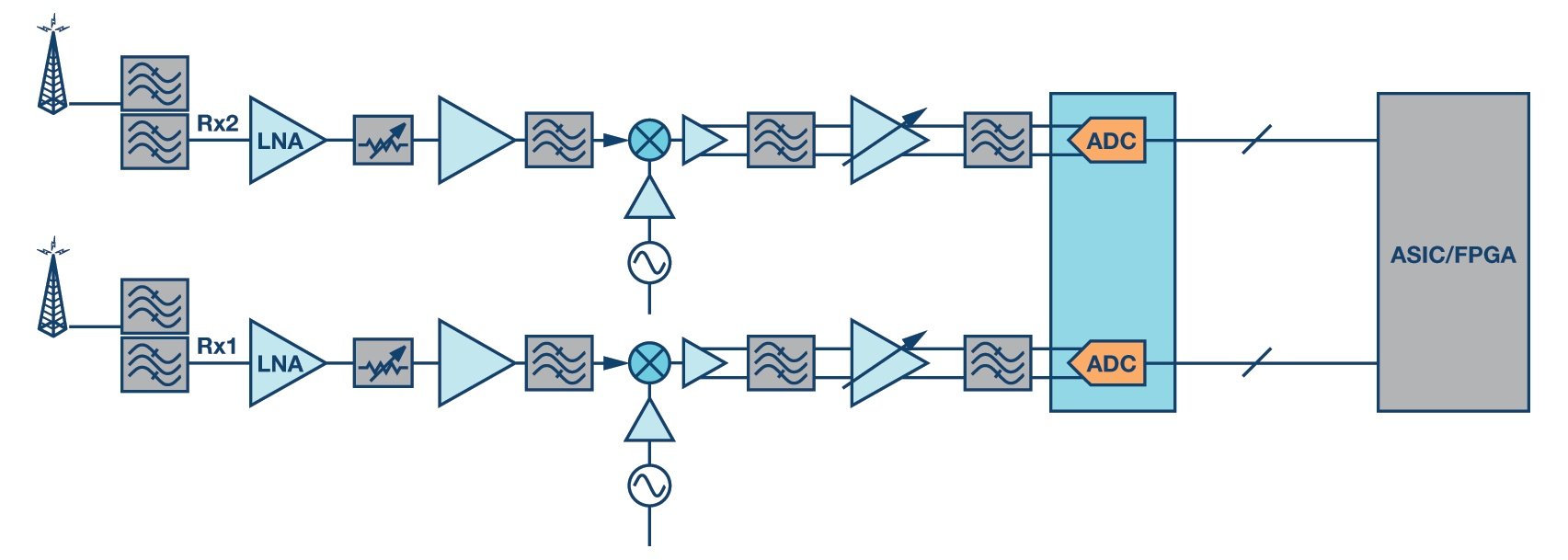
Figure 1. Traditional IF sampling receiver (Full-size image here)
The optimal way to integrate is to repartition the system to eliminate the items that cannot be integrated. Since SAW and LC filters cannot be effectively integrated, the best option is to determine how to get rid of them by re-architecting. Figure 2 shows a typical zero-IF signal chain that achieves these goals by translating the RF signal directly to a complex baseband, completely eliminating the need for an IF filter and IF amplifiers. Selectivity is achieved by introducing a pair of low-pass filters into the I/Q baseband signal chain that can be integrated as active low-pass filters instead of off chip lossy fixed IF devices. Traditional IF SAW filters or LC filters are by nature fixed while these active filters can be electronically tuned often from the hundreds of kHz range through hundreds of megahertz. Changing the bandwidth of the baseband allows the same device to cover a broad range of bandwidths without having to change a bill of material or switching between different fixed IF filters.

Figure 2. Typical zero-IF sampling receiver. (Full-size image here)
Although not intuitive from the figure, zero-IF receivers can also cover a very broad range of RF frequencies simply by changing the local oscillator. Zero-IF transceivers provide a truly broadband experience with typical coverage continuously from several hundred megahertz up to around 6 GHz. Without fixed filters, truly flexible radios are possible, greatly reducing and possibly eliminating the effort required to develop band variations of the radio design. Because of the flexible digitizers and programmable baseband filters, zero-IF designs not only deliver high performance, but also significant flexibility in adopting to a wide range of frequency and bandwidths while maintaining nearly flat performance without the need to optimize analog circuits (such as filters) for each configuration—true software-defined radio (SDR) technology. This too adds greatly to the reduction of footprint by elimination of banks of filters for applications that must cover multiple bands. In some cases, the RF filter may be completely eliminated, introducing a completely wideband radio that requires virtually no effort to change bands. By elimination of some devices and integration of others, the required PCB footprint for a zero-IF design is greatly reduced, not only simplifying the rebanding process, but also reducing the effort to change the form factor when required.
Smallest Footprint
A direct comparison of the PCB area for each of these architectures (Figure 3 and Figure 4) shows that for a dual receive path, the respective PCB area for a reasonable implementation gives 2880 mm2 (18 mm × 160 mm) for IF sampling and 1434 mm2 (18 mm × 80 mm) for zero-IF sampling. Not counting the potential elimination of RF filters and other simplifications,2 the zero-IF architecture offers the possibility of reducing the radio footprint by up to 50% as compared to current IF sampling technology. Future generation designs can potentially redouble these savings with additional integration.

Figure 3. Typical IF sampling layout (Full-size image here)
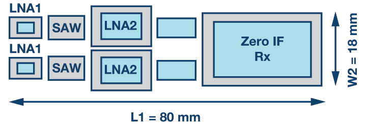
Figure 4. Typical zero-IF sampling layout (Full-size image here)
Lowest Cost
From a direct bill of material point of view, the savings when moving from an IF sampling system to a zero-IF architecture are 33%. Cost analysis is always difficult. However, a thorough examination of Figure 1 and Figure 2 shows that many of the discrete items are eliminated, including the IF and antialias filtering, and that the mixer and baseband amplifiers are integrated. What is not obvious is that because zero-IF receivers inherently offer out-of-band rejection not offered in traditional IF sampling architectures, the overall external filtering requirements are greatly reduced. There are two contributors within the zero-IF architecture that drive this. The first is the active baseband filter that provides both in-band gain and out-of-band rejection. The second is the high sample rate low-pass Σ-Δ converter used to digitize the I/Q signals. The active filter reduces the out-of-band component while the high sample rate of the ADC moves the alias point out to a sufficiently high frequency that external antialiasing filtering is not required (because the active filter has sufficiently rejected the signals).

Figure 5. Active baseband filter and ADC (Full-size image here)
By applying the baseband signals to an active filter, as in Figure 5, high frequency content is rolled off. The ADC then digitizes and ultimately filters any residual output from the low-pass filter. The cascaded results are shown in Figure 6. This figure shows what a typical receiver performance might look like with the compound effect of an active filter and Σ-Δ ADC. Shown here is a typical 3 dB desense of both in-band and out-of-band power. Note the improvement in out-of-band performance without any external filtering.
For similar levels of performance, IF sampling receivers rely on discrete IF filtering such as SAW technology for selectivity and protection from out-of-band signals and to prevent aliasing of wideband signals and noise alike from aliasing back in band. IF sampling architectures must also be protected from other unwanted mixer terms including the half-IF term, which drives additional RF and IF filtering requirements as well as restricts sample rates and IF planning. The zero-IF architecture has no such frequency planning restrictions.
Figure 6. Typical zero-IF out-of-band rejection (Full-size image here)
Depending on the design and application, this native rejection reduces or eliminates external RF filtering requirements. This results in a direct savings by their omission as external RF filters can be relatively expensive depending on the type. Secondarily, removal of these lossy devices may allow the elimination of RF gain stages, saving not only cost but reducing power and improving linearity. All of these add to the savings delivered by repartitioning and smart integration.
As noted, it is difficult to assess cost as this depends greatly on volume and vendor agreements. However, a detailed analysis shows that zero-IF architectures typically reduce the full system cost by up to ⅓ through the impact of integration, elimination, and reduction in requirements. It is important to remember that this is system cost and not device cost. Because more functions are being placed in fewer devices, some device costs may increase while overall system costs are reduced.
Beyond bill of material costs, the integrated zero-IF receiver addresses a few other areas. Because integrated systems reduce the number of devices in the system, assembly costs are lower and factory yields are higher. Because there are fewer discrete devices, alignment time is shorter. These items together reduce factory costs.
Because the zero-IF receiver is truly wideband, engineering costs are reduced to reband. IF frequencies must be carefully chosen in IF sampling systems, but with zero-IF systems, there is no careful planning required. New bands may be added largely by changing the local oscillator. Additionally because many application do not require an external RF filter when zero-IF is used, further simplifications may result. Overall, cost savings can be substantial when considering a zero-IF solution when the direct cost is considered alongside the manufacturing and engineering costs outlined above.
Lowest Power
Simply taking an architecture like that shown in Figure 1 and directly integrating it into a system on chip will not result in a power or cost savings. Power savings come through selecting an efficient architecture that can be optimized for the process on which it is targeted. Architectures like the IF sampling receiver shown involve a lot of high and midrange frequencies that are difficult to scale on low cost processes and therefore require significant amounts of power be dissipated to support the frequencies required. However, the zero-IF architecture as shown in Figure 2 works to immediately reduce the frequencies of interest to dc (baseband), allowing implementation of the lowest frequency circuits possible.
Similarly throwing bandwidth at the problem is also inefficient. Architectures like direct RF sampling provide wide bandwidths with a lot of flexibility. However, adding bandwidth to a system always adds extra power to the problem as documented by both Walden3 and Murmann.4
Unless the raw bandwidth is required, addressing the problem with bandwidth alone doesn't provide an economical solution for most receiver applications. Data from these long-term studies show two regions of converter development. The technology front documents advances in technology that provide for meaningful increases in core ac performance in the form of dynamic range and bandwidth. The architecture front documents advances in overall core architecture efficiencies. Typically the curve moves first to the right and then upward as designs are optimized. For communications applications, operation tends to be along the technology front where the slope of the line is about 10 dB per decade reduction in converter efficiency as shown in Figure 7. At this slope, doubling the bandwidth results in dissipating about three times the power. However, by the time these cores are integrated into functional devices, the efficiency has improved and typically carries a power penalty closer to 2 as it moves closer toward the architectural front.

Figure 7. Figure of merit for core ADC technology (Full-size image here)
The conclusion for applications that are concerned about power is that the lowest power solution is one where bandwidth and sample rate are optimized for the application. Zero-IF sampling with Σ-Δ converters are optimized for such applications. Depending on the specific implementation, power savings implementing a zero-IF receiver may be 50% or more reduced compared to an IF sampling architecture and as much as 120% compared to direct RF sampling.
Power is also directly related to cost. Not only does higher power drive more expensive packaging and supply generation, but for each watt a circuit dissipates, at 12 cents per kW/hr, the cost of operation is more than $1 per year per watt. Given the low cost of many electronic devices, the power to run them for just a year can easily be more than their direct cost. Thus as options for integrated radio solutions become available, applications that are sensitive to cost and power must choose the trade-offs carefully. Selecting architectures that unnecessarily increase dissipation may not only increase the power, but may also impact long-term operating costs of the solution.
Performance Enhancements
For a radio design, there are a number of key metrics that are considered important. These include specifications including noise figure (NF), linearity (IP3, IM3), desensitization, and selectivity to name a few. Beyond the normal radio specifications, there are additional specifications that are important but are often hidden from most users. These include specification distribution and drift as a function of time, supply, temperature, and process. Zero-IF architectures meet these and other key requirements for radio design.
Tracking by Temperature, Supply, and Process
One of the benefits of a fully integrated transceiver architecture is that device matching can be much better for a properly designed radio, not just initially, but devices can track effectively over process, temperature, supply, and frequency when properly designed. Any residual mismatch is readily removed with signal processing techniques that are typically embedded in these integrated solutions. While this is very typical of IC design, what is different about integration of the radio is that because all frequency dependent items are on chip with a zero-IF design, they too can be made to track. A typical radio as shown in Figure 1 includes an IF filter off chip. The characteristics of the IF filter will change as a function of time, temperature, or device to device, which will be uncorrelated to anything on chip and cannot be followed. However, one of the major advantages of integration of the filter is that because it is constructed with on-chip devices, devices can be scaled or made to ratiometrically track one another to keep performance stable. Those items that cannot be stabilized by design can easily be calibrated. The end result is that when budgeting device variations, much less margin is required than for a discrete design where all devices are uncorrelated.
For example, it is not uncommon to allocate NF variation of 1 dB for a mixer, IF filter, IF amplifier, and ADC each. When budgeting performance, these variations must be cascaded. However, in an integrated design where all critical specifications either track one another or are calibrated out, the result is a single device variation of 1 dB greatly simplifying signal chain variation. This can have a significant impact in a design as compared to a design with uncorrelated terms which would otherwise require extra system gain to offset the potential increase in noise—impacting cost, power, and linearity for the end product. In an integrated design such as that in Figure 2, the total variation in performance is considerably smaller than an uncorrelated design and therefore smaller system gain is required.
Advanced Correction Techniques
Zero-IF receivers typically have two areas that have caused concern in the past. Because complex data is generated and represented with a pair of real cascaded networks representing the real and imaginary components, errors are generated that represent gain, phase, and offset of the individual signal chains as represented in Figure 8.
Figure 8. Quadrature errors showing gain, phase, and offset terms. (Full-size image here)
These errors manifest as images in the spectrum and are what has typically prevented these architectures from being more widely adopted. However, as an integrated solution, these artifacts can be easily controlled by both analog optimization and digital correction. Figure 9 shows a typical uncorrected representation of the complex data. Here both the LO leakage (and dc offset) and image rejection (quadrature error) can be seen.
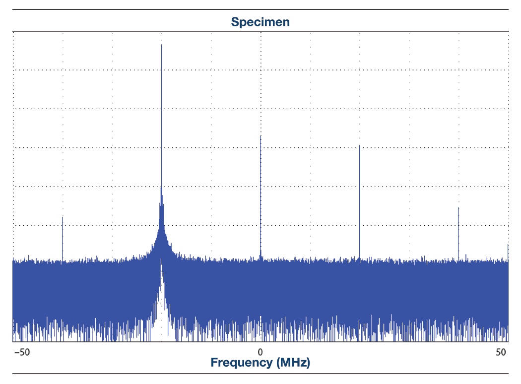
Figure 10. Typical LO leakage control (Full-size image here)
QEC
To prevent images from disrupting performance, quadrature error correction (QEC) will typically be implemented. Figure 11 shows the impact such a function can make. In this example, the image improves to better than –105 dBc, which is more than adequate for most wireless applications. For both LO leakage and QEC, tracking is employed to ensure that as performance shifts over time, the corrections stay current ensuring that optimal performance is always achieved.

Figure 11. Typical quadrature correction with LO leakage control (Full-size image here)
Quadrature error and LO feedthrough matters in a radio system. If the error is large enough, images of large blockers could mask out smaller desired signals. In Figure 12 the image of a large blocker falls at 15 MHz while a desired signal is centered at 20 MHz. If the image had fallen partly or wholly onto the desired signal, it would degrade the SNR of the desired signal resulting potentially in errors in the demodulation. Typically systems like LTE and W-CDMA have a reasonable tolerance for these kinds of images but are not totally immune. Typically these systems require image rejection of 75 dBc or better, which as shown in Figure 11 is easily met and maintained with a zero-IF architecture.

Figure 12. Example of an image blocking a desired signal (Full-size image here)
AD9371
A typical example of zero-IF transmit and receive is the AD9371. As shown in Figure 13, the AD9371 provides a high level of integrated functionality including dual transmit, dual receive along with additional functionality including an observation and sniffer receiver as well as integrated AGC, dc offset correction (LO leakage control), and QEC. The product offers wide RF coverage from 300 MHz to 6 GHz. Each transmitter can cover between 20 MHz and 100 MHz of synthesis bandwidth while each receiver is capable of between 5 MHz and 100 MHz. While this device is targeted at 3G and 4G applications, it is an ideal solution for many other general-purpose radios and software-defined applications up to 6 GHz.
![]()
Figure 13. AD9371 integrated zero-IF transceiver (Full-size image here)
The AD9371 offers a complete system integration including all of the frequency-dependent devices discussed earlier as well as all of the calibration and alignment functionality in a 12 mm × 12 mm BGA package. Adding to the receive function from Figure 4, Figure 14 includes the required transmit functionality to the footprint to yield a very compact dual transceiver design. Power depends on the exact configuration including bandwidth and features enabled, but typical dissipation of the AD9371 is only 4.86 W, including the digital functionality to maintain LO leakage and image rejection.
![]()
Figure 14. Typical zero-IF transceiver layout.
Key AD9371 Performance
Noise Figure
Figure 15 and Figure 16 show the typical NF characteristics of the AD9371. The first figure shows a broad sweep of RF frequency and that the NF is relatively flat across this spectrum. The input structure for this device is in the form of an attenuator so that the NF increases dB for dB. Assuming a worst-case NF of 16 dB with zero attenuation, allowing about 4 dB attenuation for external gain variations, a total NF of 20 dB could be assumed. An external LNA (0.8 dB) providing at least 24 dB of gain would provide a system NF of 2 dB.

Figure 15. AD9371 NF with 0 dB attenuation and 40 MHz BW (Full-size image here)
Figure 16 shows NF as a function of out-of-band blockers relative to the input of the AD9371. Assuming 24 dB of external gain, 0 dBm relative to the input of this device would occur at –24 dBm relative to the antenna connector. Considering only the impact of the AD9371, the overall NF degradation would be about 1 dB for a 3 dB degradation to the integrated receiver.

Figure 16. AD9371 NF vs. out-of-band signal power (Full-size image here)
Image Rejection
Similar to LO leakage, receive image rejection may be estimated by the information in Figure 17. With a typical input level at the antenna of –40 dBm, the image can be estimated to be better than 80 dB lower or –120 dBm relative to the antenna port.
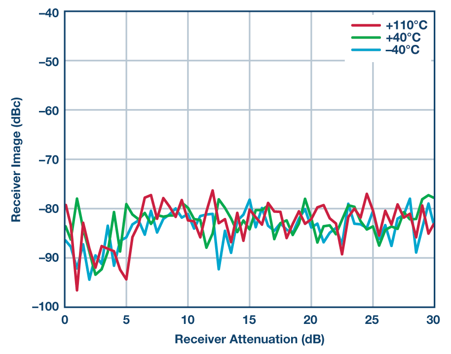
Figure 17. Receiver image rejection (Full-size image here)
Conclusion
While historically zero-IF architectures have been confined to low-performance applications, new products like the AD9371 extend zero-IF architectures to high-performance applications. Not only do these devices offer performance in line with IF sampling receivers, they go one step further by repartitioning the radio such that a more robust architecture is created that not only reduces manufacturing cost, but reduces the cost of operation once deployed. No longer does radio performance have to be compromised for a low solution cost design allowing users to focus time and resources on developing the application and not the radio implementation.
Further Reading
This article was originally published by Analog Dialogue - Visit their website to view more technical articles
References
1While this discussion primarily focuses on receivers, this discussion applies to transmitters as well. For transmitters, zero-IF has been the accepted architecture of high performance for more than a decade.
2As examined here, the typical zero-IF receiver also includes a full transmit path (AD9371) within the same package.
3R. H. Walden. "Analog-to-Digital Converters Survey and Analysis." IEEE Journal on Selected Areas in Communications, April 1999.
4Boris Murmann. "ADC Performance Survey 1997-2015." Stanford University, 2015.
Related Content