Facebook
 Google
 GitHub
 Linkedin
Around the Industry: Examples of How Complex ICs Require Complex Design Tools
Industries like aerospace and defense are only raising the bar on IC requirements. Here are a few recently announced tools helping IC designers meet the task.
The U.S. Department of Defense (DoD) recently announced that as it enters the second phase of its RAMP project—the Rapid Assured Microelectronics Prototypes—it has selected both Microsoft and Qualcomm to develop ICs.
The primary aim of the RAMP project is to create reliable, secure, and advanced microelectronic designs for national security and defense applications. The DoD also hopes RAMP will promote teamwork among other commercial and defense industrial base (DIB) leaders, such as Cadence, Cliosoft, Flex Logix, GlobalFoundries, and Intel.
RAMP is but one example of the programs underway to develop ASICs for industries spanning telecommunication, IoT, healthcare, automotive, data processing, and satellite communication. To accommodate these complex chips, many companies have developed modules, software, and verification tools to smooth the design process.
Here are a few examples of recent tools that may help engineers in this dynamic field.
The "Industry's First" eFPGA Soft IP Yields Design Flexibility
The notion behind Intellectual Property (IP) blocks is familiar to most engineers: designers can use pre-existing building blocks to speed up product development while minimizing risks and costs. Owners of these reusable IP blocks can license them for third-party use.
Designers can opt for soft or hard IP blocks in ASIC/system-on-chip (SoC) designs depending on whether they need a more flexible hardware description language (HDL) code or an already pre-mapped, fixed, and tested final hardware layout, respectively.
Menta recently announced a so-called industry first: a soft IP embedded field-programmable gate array (eFPGA). The company claims this solution offers designers unprecedented flexibility, implementation control, and low costs for ASIC and SoC designs.

Menta's eFPGA IP solution. Image used courtesy of Menta
Additionally, the eFPGA-based IP is said to allow post-manufacture product modification, offering end product upgradeability. Using such soft IP blocks, Menta says, will minimize overall design costs since designers are assured efficient implementation regardless of foundry and EDA tool.
Both soft and hard IP blocks offer several benefits and limitations. For one, soft IP blocks are highly flexible in product development and implementation. In contrast, designers cannot significantly alter hard IP block designs at functional levels. This is because hard IP block vendors incorporate chip functionalities into the electronic wafers themselves.
However, soft IP block vendors offer zero to little support or warranty for altering block designs. Hard IP blocks vendors, on the other hand, guarantee higher performance because of the extensive tests and support in several foundries and silicon nodes.
As Menta's new solution demonstrates, users can map soft IP blocks to any foundry on a standard cell technology node. This flexibility allows customers to physically implement IP blocks in their environment using an electronic design automation (EDA) tool.
How Modules May Accelerate ASIC Design
It's a common industry practice to reuse IP in several implementations. However, designers who wish to customize block interfaces are often bottlenecked because there is currently no global standard for IP block interfaces. A standardized platform wouldn't only reduce design time; it would significantly minimize overall design costs and facilitate a product's adoption and commercialization.
Although several providers have attempted to create a platform with such standardized, reusable IP blocks, none have successfully developed one that can be implemented across several application areas.
Now, ASIC consultant Sondrel has recently released an IP platform family—dubbed "Architecting the Future"—which is said to allow designers to customize and implement standardized IP block interfaces. This platform is based on Sondrel's Scalable Architecture Framework (SAF)—a modular approach that allows Sondrel to choose an appropriate IP platform for any given customer and customize it by adding more computing blocks.
The company created this platform by integrating blocks that meet performance and functionality requirements of specific application areas, including video and data processing, advanced driver assistance systems (ADAS), and edge IoT data processing.

Sondrel says its Architecting the Future IP solution can be especially beneficial in automotive applications. Image used courtesy of Sondrel
These solutions include reusable modular IP blocks with individual "wrappers" that contain a standardized set of functions and interfaces. Sondrel says the use of wrappers for IP blocks is novel in and of itself, saving up to 30% design time and significantly minimizing design costs and risks.
By encapsulating IP blocks, the wrappers support several functions and services, including clock reset and power management. Sondrel claims it can rapidly create new wrappers for any third-party IP block—the result being quick-to-market products.
Speed Adapters Pick Up the Pace for SoC Validation
Memory and PCIe speed adapters can help engineers efficiently integrate FGPA prototypes with native system platforms. This integration enables validation performance at system run speeds.
Avery Design Systems, in partnership with FPGA prototyping solutions developer S2C, recently pitched a new way to validate data center and AI/ML SoCs. This method integrates PCIe 6.0, LPDDR5, and HBM3 speed adapters with FPGA prototyping solutions.
Avery Design Systems and S2C say their proposed technique can efficiently handle the performance limitations of multi-FPGA representations of SoCs. Moreover, the partnership aims to address the growing performance requirements and complexities of large-scale SoC designs by using accurate and rapid verification methodologies.
By integrating memory and PCIe speed adapters with a high-density FPGA platform, the two companies say they can enable designs to meet capacity and performance requirements in complex SoC designs.

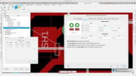
Diagram of Avery's PCIe speed adapter in an FPGA prototyping system. Image used courtesy of Avery Design Systems
Some key capabilities of memory speed adapters from Avery include:
- Support for a wide range of interfaces, including HBM2E, HBM3, DDR4, LPDDR4, LPDDR5, and SoT
- MCU-controlled log file debugging
- Synthesis, simulation, and timing scripts inclusion
Avery also offers PCIe speed adapters that include:
- Multiple lane widths
- Physical layer initialization
- Root Complex (RC) and Endpoint (EP) independent configurations
- Low pin-count interfaces
- Support for several PIPE data widths and PIPE rates
Avery believes that FPGA prototyping and SoC validation based on interconnect and memory technology is on the horizon.
IC Designers Have More Tools at Their Fingertips
Chips are only getting smaller and more complex. Earlier this month, AST SpaceMobile underscored this point when it tapped EnSilica to develop ASICs for its cellular broadband network.
As a response to the challenges of modern chip design, industry players have developed design tools that may significantly reduce design time, costs, and risk. Some of these tools include EDA tools, soft IP blocks, high-speed adapters, and even IP block wrappers.
Related Content