Facebook
 Google
 GitHub
 Linkedin
Digitally Adjust DC-to-DC Voltage Regulators: A PMBus-Controlled Current DAC
A PMBus-controlled, bidirectional current DAC (digital-to-analog converter) that can adjust the output voltage of a DC/DC converter.
A PMBus-controlled, bidirectional current DAC (digital-to-analog converter) that can adjust the output voltage of a DC/DC converter.
Linear Technology, now owned by Analog Devices, recently announced the LTC7106. This small IC (10-lead, 3 × 2 mm) is a 7-bit bidirectional current-output DAC that can be used to control the output voltage of, according to the datasheet, "the vast majority" of power management controllers and DC/DC voltage regulators, including buck and boost regulators. It does this by sinking or sourcing current in such a way as to adjust the voltage applied to the regulator’s feedback pin.
This dynamic VOUT control could probably come in handy in a wide variety of applications, including test/verification applications such as voltage margining.
_typical_diagram.jpg)
Figure 1. A typical LTC7106 application. Diagram taken from the datasheet (PDF).
PMBus/I2C-Interface Compliant
The LTC7106 is controlled via a PMBus (or power management bus) interface. The PMBus is a standardized communications protocol used in power systems; it’s a two-wire interface that is similar, but not identical, to the SMBus (system management bus). And although you may not be familiar with either of these protocols, you are probably very familiar with I2C, which both PMBus and SMBus are built upon.
For a summary of the similarities between these three interface standards, take a look at the section entitled Operation on page 11 of the datasheet.
Controlling the Regulator's Output Voltage
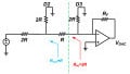
Upon receiving the 7-bit DAC code via its PMBus interface, the LTC7106 converts this digital value into the corresponding current, which can be either a positive current (flowing out of the IDAC pin) or a negative current (flowing into the IDAC pin); this is why the device is described as a bidirectional current-output DAC. When connecting the IDAC pin to the feedback node of a voltage regulator, the regulator's VOUT is set according to the following equation (see the figure below):
$$V_{OUT}=V_{REF}*\left(1+\frac{R_{FB1}}{R_{FB2}}\right)-I_{DAC}*R_{FB1}$$
where
VREF = the reference voltage of the voltage regulator,
RFB1 and RFB2 are the resistances of the feedback resistors, and
IDAC = the programmed current (see Table 2 on page 8 of the datasheet).
_typical_diagram_-_Copy.jpg)
Figure 2. According to the datasheet, the voltage regulator's VOUT is determined by the regulator's VREF value, the LTC7106's IDAC current, and the resistances RFB1 and RFB2.
So what is really going on here? The converter’s feedback pin is an input, and the voltage applied to this input is part of a feedback system that controls the magnitude of the output voltage. Usually, we have a resistive divider that is designed so as to produce the desired feedback voltage.
How does a current DAC change the feedback voltage, considering that the resistances don’t change?
Well, normally, the same current flows through both resistors, and the divider’s output voltage is this current multiplied by the lower resistance. With the DAC involved, this is no longer the case. Notice in the above diagram how the lower resistor is kind of in parallel with the IDAC line. This means that the current flowing through the upper resistor is shared between the lower resistor and the DAC. When the IDAC pin is sinking current, you can think of the DAC as a programmable resistor in the sense that it opens up a variable current path from the “VREF” node to ground. This programmable “resistance” is in parallel with the lower resistor; by varying the current, you are effectively varying the equivalent resistance of the lower half of the divider, and changing the equivalent resistance produces corresponding changes in the feedback voltage.
As mentioned previously, the LTC7106 works with both buck and boost regulators. The two figures below display start-up characteristics and margining functionality for a step-up regulator and a step-down regulator. Note that the margin-high/margin-low behavior varies according to the values stored in the margining registers.
_buck_regulator.jpg)
Figure 3. Start-up and margining with a buck regulator, from the datasheet.
_boost_regulator.jpg)
Figure 4. Start-up and margining with a boost regulator, from the datasheet.
Keep in mind that the accuracy, over the IC's full operating temperature range, of the IDAC positive output current is better—by about a factor of two—than that of the negative output current (see the figure below):
- IDAC positive output current: ±0.8% accuracy (from -40°C to +125°C)
- IDAC negative output current: ±1.5% accuracy (from -40°C to +125°C)
_IDAC_temperature.jpg)
Figure 5. The PIDAC (positive IDAC) output current has better accuracy, over temperature, than the NIDAC (negative IDAC) output current. Plots taken from the datasheet.
Programmable Slew Rate
The LTC7106 includes a programmable slew rate controller that prevents excessively abrupt changes to the regulator’s output voltage. It would be interesting to know what exactly might happen if the slew rate weren’t limited. Could a rapid change introduce instability into the regulator’s feedback system, or is it simply a matter of preventing potentially stressful (for the powered components, not the designer) variations in supply voltage? In any event, this is a good feature.
Have you had an opportunity to use this new output-voltage-controlling DAC? If so, leave a comment and tell us about your experiences.