Facebook
 Google
 GitHub
 Linkedin
Infineon Tackles High-frequency Switching Losses With Latest OptiMOS 6 MOSFETS
With increased performance of drain-source on-state resistance, gate charge, and figures of merit, Infineon's latest 100 V MOSFET technology seeks to improve high-frequency switching applications.
With the growing demand for high efficiency and reliability in many power applications, like switched-mode power supplies (SMPS) and battery-powered electronics, semiconductor manufacturers are developing advanced power metal-oxide-semiconductor field-effect transistor (MOSFET) technologies to meet this demand.
Hoping to meet this demand, one leading company, Infineon, has recently announced the release of its OptiMOS 6 100 V power MOSFET technology.

The two versions of OptiMOS 6 MOSFET solution. Images [modified] used courtesy of Infineon
This article will give an overview of this novel technology, explore key improvements, specifications, applications, and its benefits to switching operations.
Overview of OptiMOS 6 100 V MOSFET Technology
The latest product release from Infineon features its OptiMOS 6 100 V power MOSFET technology, which promises record-high standards for high-frequency switching applications.
In line with the drive to promote cleaner energy at Infineon, the company builds solutions for energy optimization and high power density in electrical power transmission, consumption, and storage.
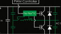
The OptiMOS 6 power MOSFET further emphasizes this drive by offering improved drain-source on-state resistance (RDS(ON)), gate charge (Qg), and figures of merit (FOM) values, which can be important for energy loss minimization in high switching frequency applications, such as telecommunication and solar powering.
Overall, this Infineon solution claims to be well-suited for battery management systems (BMS) and battery-powered applications (BPA) due to its expanded safe operating area (SOA) and "industry-best" RDS(ON).
Infineon leveraged its novel design concept to improve RDS(ON) and FOM values in the OptiMOS 6 solution.
These value improvements offer several benefits to high-frequency applications, including:
- High efficiency
- System cost reduction
- Long equipment lifetime
- Improved power density
- Simpler thermal designs
- Minimized paralleling
When compared to the existing OptiMOS 5 technology, this new solution offers 18% RDS(ON) reduction and 29% and 42% improvements in FOM and gate-to-drain charge FOM (FOMgd), respectively. This technology, which comes in a small footprint, SuperSO8 5x6 and PQFN 3.3 x 3.3 packages, can achieve higher efficiencies than the OptiMOS 5 technology, with energy consumption and cost-saving potential.
Overall, this product claims to pack quite a bit of technology and improvements into a small package. With that being said, let's take a look at the applications.
New Standards for High Switching-Frequency Applications?
As stated, the RDS(ON), Qg, and fFOM are some key parameters that determine the performance of MOSFET technologies in high switching frequency applications.
OptiMOS 6 solutions could offer significant improvements across these parameters, claiming the industry-highest standards for switching applications.
RDS(ON) for OptiMOS 6
RDS(ON) is the on-state resistance measurement between the drain and source terminals of the MOSFET. This parameter is proportional to conduction losses: a reduction RDS(ON) results in a corresponding reduction in conduction losses.
A lower RDS(ON) also offers additional benefits, including electronic components paralleling minimization, lesser PCB real estate, and cost-saving, which ultimately leads to a corresponding increase in power density.

OptiMOS 5 vs. OptiMOS 6: RDS(ON) reduction. Image used courtesy of Infineon
Gate Charge
While Qg is the amount of charge required to drive (or turn on) the MOSFET, the gate-to-drain charge (Qgd) is the portion of the gate charge needed to complete drain voltage transitions. Note that these two parameters are essential to switching loss reduction in high-frequency switching and hard-switching applications. Lower Qg and Qgd values are desirable since they result in switching loss reductions.

OptiMOS 5 vs. OptiMOS 6's gate charge reduction. Image used courtesy of Infineon
Figure of Merit
The FOM accounts for both conduction and switching losses when evaluating the performance of a technology. This performance indicator is a product of the drain-source on-state resistance and the gate charge.
Since this parameter accounts for both losses, it offers designers a more comprehensive view of the performance of technology at a glance. Moreover, gate-to-drain charge FOM also accounts for both losses but at MOSFET turn-off-state.
By achieving lower values for these parameters, Infineon sets new standards for switching and conduction losses in high-frequency switching applications.
Features and Benefits of OptiMOS 6 Tech
OptiMOS 6 solution offers several capabilities beneficial to a wide range of applications.
The solution achieves significant efficiency improvements, cost reductions, and overall performance with 18%, 29%, and 42% improvements in RDS(ON), FOM, and gate-to-drain charge FOM (FOMgd), respectively improvements.
Key benefits OptiMOS 6 MOSFET technology offers high-frequency switching applications include:
- low switching and conduction losses
- high reliability
- increased power density
- minimized electronic component paralleling
- high efficiency
- environmental friendliness
High-frequency switching applications are known for switching and conduction losses. However, with this new Infineon solution, designers could potentially minimize losses and high-efficiency operations.
Related Content