
 Facebook
 Google
 GitHub
 Linkedin
MAX232: The Single-Supply Transceiver That Shrunk RS-232 to One Chip
Introduced in the late 1980s, Maxim’s MAX232 made RS-232 interfaces trivial with dual drivers, dual receivers, and their +/-10 V rails—all from a single +5 V supply.
When the MAX232 arrived from Maxim Integrated in the late 1980s, serial ports were still standard on microcomputers and industrial gear, but supporting them was a headache. RS-232 called for positive and negative voltages, typically around +/-12 V, and legacy drivers like the MC1488/1489 pair demanded bipolar supplies that no longer existed in the emerging world of single-rail, +5 V digital logic.
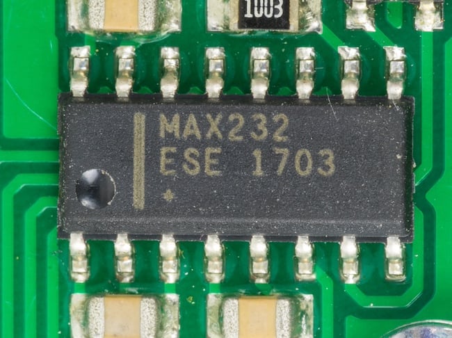
A MAX232 chip in a DIP-16 package. Image used courtesy of Raimond Spekking via Wikimedia Commons (CC BY-SA 4.0)
The MAX232 solved that problem by integrating both transmit and receive channels and generating its own +/-10 V rails using nothing more than four external capacitors. That combination turned an awkward analog interface into a drop-in block. It made full-voltage RS-232 accessible to small boards, microcontroller systems, and embedded products without dedicated power rails. And it defined a function that countless clones and derivatives still follow today.
Folding a Bipolar Port Into One Package
The MAX232’s importance is easier to appreciate by looking at what it replaced. Classic RS-232 designs used separate driver and receiver chips—typically bipolar line drivers for the positive and negative swings and comparators for the incoming signals—all powered from regulated +/-12 V rails. That architecture dated back to the minicomputer era, when multiple supplies were common, and RS-232 was still considered a long-haul electrical interface rather than a simple point-to-point serial port.
By contrast, the MAX232 ran entirely from +5 V. Internally, a pair of switched-capacitor pumps doubled the supply to create an unregulated +10-V rail and inverted it to make -10 V, enough to satisfy RS-232’s requirement that logic “1” be negative and logic “0” be positive. Two driver stages took TTL or CMOS inputs and shifted them into the RS-232 domain, complete with the inverted polarity the standard expects. On the other side, two receiver channels accepted inputs anywhere from about +/-3 V up to +/-25 V and produced clean 5 V logic outputs.
The part arrived at a time when embedded gear was slimming down its power supplies, and the ability to achieve a full-compliant RS-232 link from a single logic rail was a breakthrough. Unlike earlier designs, the MAX232 needed no external regulation for its pump rails and no bias networks to set its thresholds. As long as the capacitors met the datasheet’s value and ESR requirements—1 µF originally, 0.1 µF in the later MAX232A—it generated stable +/- line voltages and drove standard RS-232 loads at speeds up to roughly 120 kbit/s.
This integration made the MAX232 a natural fit for microcontroller-to-PC links, test equipment, modem interfaces, and industrial hardware that needed RS-232 levels but didn’t require a dedicated dual-supply stage. It effectively reduced the entire interface to one IC footprint and four off-the-shelf capacitors.
Charge Pumps, Receivers, and Drivers at Work
Inside the device, the architecture was deceptively straightforward. The charge-pump section consisted of two oscillator-driven switches feeding a pair of flying capacitors. One stage doubled +5 V to around +10 V, and the other inverted that rail to produce -10 V. Two reservoir capacitors stabilized each output. None of these rails was meant as general-purpose supplies; their job was simply to keep the RS-232 voltages within spec across a compliant load.
Each transmitter channel used these rails to produce the correct bipolar output swing. Under load, the voltages sagged slightly, but still stayed above RS-232’s minimum +/-5 V requirement at the remote end of a cable. Short-circuit protection and current limiting prevented the driver from overloading when miswired or plugged into unconventional serial hardware.
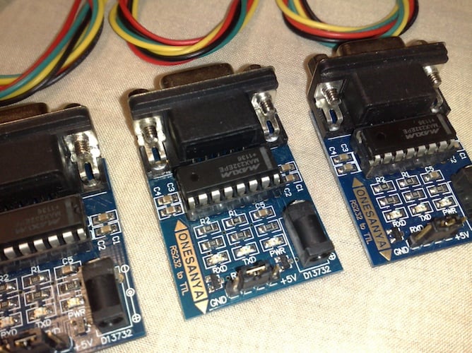
RS-232 to TTL converters using the MAX232. Image used courtesy of Dsimic via Wikimedia Commons (CC BY-SA 3.0)
On the receive side, each input fed a comparator with built-in hysteresis. That gave the MAX232 surprising immunity to slow or noisy edges, mains-induced interference, and the sometimes-questionable cabling practices found in industrial environments. As long as the incoming signal crossed roughly +/-3 V, the receiver produced clean TTL-level transitions with enough margin to satisfy downstream logic.
This architecture allowed the MAX232 to tolerate wiring mistakes and the unpredictable signalling common in long-used serial ports. It was, in many ways, the RS-232 equivalent of the µA741’s approach to op amps: integrate just enough internal behavior to make an awkward analog job simple and predictable.
A Template That Never Went Away
The MAX232’s impact mirrors the staying power of the CD4000 family and the ubiquity of the 741. Like those devices, it distilled a class of circuitry into a single, reusable abstraction.
Once Maxim proved that a charge-pump-powered RS-232 transceiver was viable, it became the standard model. Variants came quickly, with the MAX232A reducing the capacitor size to 0.1 µF, MAX202-class parts improving ESD protection, and MAX3232-type devices extending the concept to 3.3 V systems. Second sources from nearly every major analog vendor followed, making “MAX232-compatible” a functional description.
Even as USB displaced RS-232 in consumer hardware, the MAX232 and its successors continued to appear in embedded designs, industrial controllers, CNC systems, laboratory instruments, and telecom gear. Many of these environments still use DB9 connectors and long cable runs, where RS-232’s high noise margins and simple point-to-point protocol remain big selling points.
Like Intel’s 1103 DRAM and the 2708 EPROM—each defining a function that others would iterate on for decades—the MAX232 created a stable interface model that outlasted the era in which it was produced. It continues to ship today because it solves the same problem just as cleanly today as it did when it arrived.
Related Content










the chips that made my life easier and the bedrock of designs , all mentioned
741, an op amp that “just worked”
ne555, timer / charge pump that just worked
max232, just so robust and worked
only niggle I ever had with max232, was the -10 and -5 pins being right next to ttl / cmos pjns. number of times we used to slip when using a scope to debug signals,