 Facebook
 Google
 GitHub
 Linkedin
One-Nanometer Transistor Keeps Moore’s Law Relevant Another Year
Researchers at the Department of Energy's Lawrence Berkeley National Laboratory have created the world's first 1nm gate.
Researchers at the Department of Energy's Lawrence Berkeley National Laboratory have created the world's first one-nanometer transistor gate.
It's no secret that modern research has been vested into reducing the size of electronic components. But how small these new transistors are may even shock industry researchers.
Our modern world of electronics has been achieved due to one remarkable trend: the constant quest to reduce the size of metal oxide semiconductor field effect transistors—MOSFETs.
This component is what is used to amplify and switch electronic signals and is essentially the foundation of most integrated circuits. In the last fifty years, MOSFETs have shrunk down from a few micrometers in size to just 20 nanometers, nearly a thousand-fold smaller.
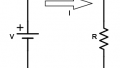
Unfortunately, conventional silicon electronics have been approaching a fundamental limit to their size. This is due to quantum effects that occur as silicon approaches a gate length of five nanometers, causing unpredictable behavior that significantly inhibits their ability to function reliably. This effect is known as quantum tunneling, where an electron is capable of passing through barriers and is increasingly likely to do so as the barrier size gets smaller.
Companies such as Intel have announced that their intention to research alternative materials to replace silicon once 7nm-length gates were achieved last year. They've now been succeeded by DOE researchers.

A visualization of quantum tunneling. Image courtesy of IEEE Spectrum.
Developing the World's Smallest Transistor Gate
Earlier this month, a research team led by Ali Javey at Lawrence Berkeley National Laboratory created the first working transistor with a one-nanometer gate. The breakthrough was accomplished when the team created a two-dimensional MOSFET using a material called molybdenum disulfide (an alternative to silicon) and a single-walled carbon nanotube as a gate instead of assorted metals. Carbon nanotubes have been the subject of intensive research for years now and recently outperformed silicon in transistors.
The material, MoS2—which has found use in multiple applications across the industry—has quite handily offered a solution to the problem that silicon has with its fundamental limitations. Electrons in MoS2 molecules will act as if they are heavier than those in silicon molecules. This causes the electrons to move more slowly which, in turn, makes them much easier to control.
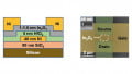
![]()
A representation of the molybdenum disulfide channel and 1-nanometer carbon nanotube gate. Image credit: Sujay Desai/UC Berkeley
Silicon is actually preferable to MoS2 as a channel material in most cases where the electrons will encounter less resistance as they pass through the material. But miniaturizing past the 5nm point with silicon inhibits the gate from preventing electrons that will pass through to the drain, preventing the transistor from switching to off.
The gate was reconstructed using carbon nanotubes due to a reevaluation of materials. Knowing that traditional lithography approaches were not applicable at this scale, the research team instead looked to use carbon nanotubes.
The team was able to measure a device and showed that the new 1nm-thick transistor was capable of controlling electron flow. Including the wiring, the entire device is larger than 1nm and the circuit is altogether functional.
A Realistic View of Nano-Sized Transistors
Amidst the hype of creating the world’s first functioning 1nm gate, the researchers have advised people not to get overly eager to see the new transistor anytime soon.
The paper's lead author, Ali Javey, describes this 1nm gate as "a proof of concept." The process of creating the gate will need to be repeated many, many times before it can even be truly optimized for efficiency. After that point, it will need to be developed further and attached to chips. All of this will likely take years.
In the meantime, however, this step is extraordinarily important because it breaks the five-nanometer limit that silicon places upon transistors.
With this new advancement, Javey says, we can still apply Moore's Law and look to the future of tech with optimism.
The original research paper was published in the AAAS journal, Science.


I wonder at what point a single cosmic ray disintegration will cause the transistor to erroneously conduct and crash the computer!
Great explanation, great article. Thanks!