Facebook
 Google
 GitHub
 Linkedin
Examining the Unbalanced Loading Effect of a Difference Amplifier on a Bridge Circuit
In this article, we’ll see that in addition to having high common-mode rejection, in-amps should provide high and equal input impedances.
In a previous article, we discussed that instrumentation amplifiers (in-amps) should have a high common-mode rejection to successfully extract a small differential signal. In this article, we’ll see that in addition to having high common-mode rejection, in-amps should provide high and equal input impedances. We’ll also examine the loading effect of a difference amplifier on a resistive bridge to gain more insight into this requirement of in-amps.
An In-Amp Should Provide High, Balanced Impedance at Its Inputs
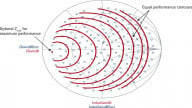
The block diagram of a two-element varying bridge measurement system is depicted in Figure 1.
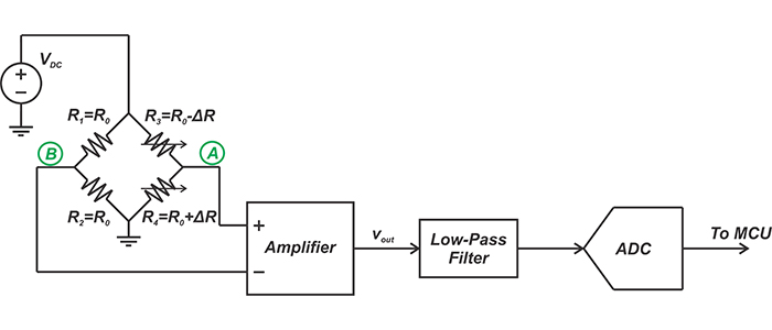
Figure 1
Applying Thevenin's theorem, we can model the bridge as shown in Figure 2.
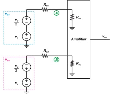
Figure 2
Here, \(R_{th1}\) and \(R_{th2}\) are the equivalent resistances of the two bridge branches. Besides, the overall Thevenin equivalent voltages of nodes A and B, \(V_{th1}\) and \(V_{th2}\), are decomposed into differential (\(v_d\)) and common-mode (\(v_c\)) components given by:
\[v_c= \frac{v_{th1}+v_{th2}}{2}\]
\[v_d= v_{th1}-v_{th2}\]
The above figure models the impedances “seen” at the amplifier inputs by \(R_{in1}\) and \(R_{in2}\). Let’s see how unequal input impedances (\(R_{in1} \neq R_{in2}\)) affect the circuit operation. Assume that the bridge is balanced and the resistor values are as shown in the following figure.
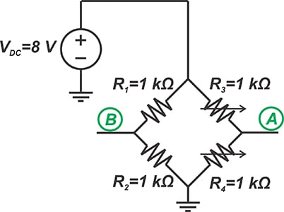
Figure 3
In this case, the values of the Thevenin equivalent circuit can be found as: \(v_d\)=0, \(v_c\)=4 V, and \(R_{th1} =R_{th2} =500 \Omega \).
Moreover, suppose that the employed amplifier has unequal input impedances (\(R_{in1} \neq R_{in2}\)) and we have \(R_{in1}=10 k \Omega\) and \(R_{in2}=10.5 k \Omega \). Two important observations can be made:
Observation 1— Considering the equivalent model in Figure 2, we have:
\[v_A=\frac{R_{in1}}{R_{in1}+R_{th1}} v_c= \frac{10~k \Omega}{10~k \Omega + 500~\Omega} \times 4~V = 3.8095~V\]
\[v_B=\frac{R_{in2}}{R_{in2}+R_{th2}} v_c= \frac{10.5~k \Omega}{10.5~k \Omega + 500~\Omega} \times 4~V = 3.8181~V\]
While the bridge was initially balanced (\(v_A = v_B\)), unequal input impedances of the amplifier cause unequal loading effects on the two branches and lead to an unbalanced bridge (\(v_A \neq v_B\)).
Observation 2— Assuming that the amplifier can completely reject any common-mode signals, i.e., \(A_{cm}=0 \), and has a differential gain of \(A_d=20\), we can find the output voltage as:
\[v_{out}=A_d \times \left (v_A-v_B \right )=20 \times \left (3.8095-3.8181 \right )=-172~mV\]
While the amplifier was assumed to have infinite common-mode rejection ratio (CMRR), the unbalanced loading effect of the amplifier allows the common-mode voltage to produce an error signal at the output. This effect will be even more serious if we use an amplifier with lower input impedances.
Hence, in addition to having high common-mode rejection, the amplifier should provide high and equal impedances at its inputs.
Unbalanced Loading Effect of a Difference Amplifier
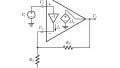
We can use a difference amplifier, depicted in Figure 4 with some typical resistor values, as the bridge amplifier. It can achieve a high CMRR; however, its input impedances are limited and unequal.
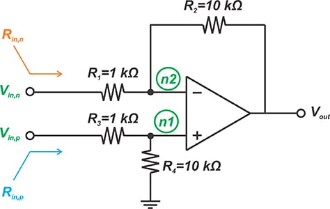
Figure 4
The impedance of the non-inverting input (\(R_{in,p}\)) is:
\[R_{in,p}=R_3 + R_4 \]
Equation 1
The impedance of the inverting input (\(R_{in,n}\)), assuming that the non-inverting input is grounded, can be found as:
\[R_{in,n}=R_1\]
Equation 2
With the resistor values given in Figure 4, \(R_{in,n} =1~k \Omega \) that is eleven times smaller than the resistance of the non-inverting input (\(R_{in,p}=11~k \Omega\)).
Assume that, as shown in Figure 5, we connect the above difference amplifier to our bridge circuit.
Can we use Equations 1 and 2 to assess the loading effect of the difference amplifier on the bridge circuit?
It is important to note that only the equation for the non-inverting input is valid in general. The equation for the inverting input, Equation 2, is obtained under the assumption that the non-inverting input is grounded. In other words, the impedance of the inverting input depends on the voltage applied to the non-inverting input (\(V_{in,p}\)). This is due to the fact that \(V_{in,p}\) determines the voltage that appears at nodes n1 and n2. This, consequently, affects the current drawn by the inverting input of the difference amplifier.
Some documents, such as “The Designer's Guide to Instrumentation Amplifiers” from Analog Devices, mention Equations 1 and 2 when discussing the unbalanced loading effect of a difference amplifier on a bridge circuit without highlighting that we are not actually allowed to use the above equations when analyzing a bridge circuit.
I believe such documents mention Equations 1 and 2 only to give us a sense about the unbalanced loading effect of the difference amplifier.
It can be shown that, with arbitrary inputs applied to a difference amplifier, \(R_{in,n}\) is given by the following equation:
\[R_{in,n}= \frac {R_1}{1- \frac {R_4}{R_3+R_4} \times \frac {V_{in,p}}{V_{in,n}}}\]
where \(V_{in,p}\) and \(V_{in,n}\) are the voltages at the inverting and non-inverting inputs of the amplifier, respectively. For example, with \( \frac{V_{in,p}}{V_{in,n}}=-1\) and the resistor values shown in Figure 4, we obtain:
\[R_{in,n}= \frac{R_1(R_3+R_4)}{R_3+2R_4}=\frac{1~k\Omega \times \left ( 1~k\Omega + 10~k \Omega \right )}{1~k \Omega + 2 \times 10~k \Omega} = 523.8~\Omega\]
that is almost half the value given by Equation 2 (1 kΩ). Another interesting case is \( \frac {V_{in,p}}{V_{in,n}}=1 \) that leads to:
\[R_{in,n}= \frac {R_1}{1- \frac {R_4}{R_3+R_4}}= \frac {1~k\Omega}{1- \frac {10~k\Omega}{1~k \Omega+10~k\Omega} } =11~k \Omega\]
This is equal to the resistance of the non-inverting input \(R_{in,p}\). With many bridge circuits, the voltages at nodes A and B are close to each other (\(\frac {V_{in,p}}{V_{in,n}} \approx 1 \)); therefore, \(R_{in,n}\) will be close to \(R_{in,p}\).
In other words, although a difference amplifier does have unequal loading effects on the two branches of a bridge circuit, the difference in \(R_{in,n}\) and \(R_{in,p}\) is not as large as that predicted by Equations 1 and 2.
Examining the Loading Effect of a Difference Amplifier on a Bridge Circuit
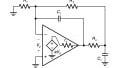
In this section, we’ll use the example circuit shown in Figure 5 to discuss how we can calculate the loading effect of a difference amplifier on a bridge circuit.
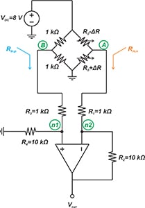
Figure 5
We’ll consider two different cases: a balanced bridge with \(R_0=1~k\Omega \) and \(\Delta R=0 \) and an unbalanced bridge where \(R_0=1~k \Omega\) and \(\Delta R=10~\Omega\).
Case 1— Balanced Bridge with \(R_0=1~k \Omega \) and \( \Delta R=0 \)
The negative feedback along with the high gain of the op amp will force both nodes n1 and n2 to be at the same potential. Since the resistor values and the node voltages are the same for both sides of the bridge, we can conclude that \(v_A = v_B\).
This result is also consistent with the discussion of the previous section: when both the inverting and non-inverting inputs of a difference amplifier are at the same potential (\( \frac {Vin,p}{Vin,n} \approx 1\)); the amplifier exhibits equal resistances at its inputs (\(R_{in,n}=R_{in,p}\)) leading to a balanced loading effect on both sides of the bridge.
Case 2— Unbalanced Bridge with \(R_0=1~k \Omega\) and \(\Delta R=10~\Omega\)
First the easy part, the impedance of the non-inverting input (\(R_{in,p}\)) is:
\[R_{in,p}=R_3+R_4=1~k\Omega + 10~k\Omega=11~k\Omega\]
Therefore, the voltage of node B can be found as:
\[v_B=\frac {(R_{in,p}||1~k\Omega)}{(R_{in,p}||1~k\Omega)+1~k\Omega}\times 8~V= \frac{0.9167~k\Omega}{0.9167~k\Omega +1~k\Omega} \times 8~V=3.8261~V\]
In the above equation, \(R_{in,p} ||1~k\Omega \) denotes the parallel equivalent resistance of \(R_{in,p}\) and \(1~k\Omega\). To calculate \(v_A\), we need to find \(R_{in,n}\) that is given by:
\[R_{in,n}=\frac{R_1}{1-\frac{R_4}{R_3+R_4} \times \frac{V_{in,p}}{V_{in,n}}}= \frac {1~k\Omega}{1-\frac{10~k\Omega}{1~k\Omega + 10~k\Omega}\times \frac {V_{in,p}}{V_{in,n}}}\]
Substituting \(V_{in,p}=v_B=3.8261~V\) and \(V_{in,n}=v_A\), we obtain:
\[R_{in,n}=\frac {1~k\Omega}{1-\frac {10}{11} \times \frac{3.8261}{v_A}}\]
Equation 3
The voltage at node A can be found as:
\[v_A=\frac{(R_{in,n}||1.01~k\Omega)}{(R_{in,n}||1.01~k\Omega)+ 0.99~k\Omega} \times 8~V\]
Substituting Equation 3 into the above equation gives \(v_A=3.8528~V\).
We can use LTspice to verify these calculations. The schematic is shown in Figure 6. As you can see, the OP1177, a precision operational amplifier from Analog Devices, is used instead of the ideal op-amp.
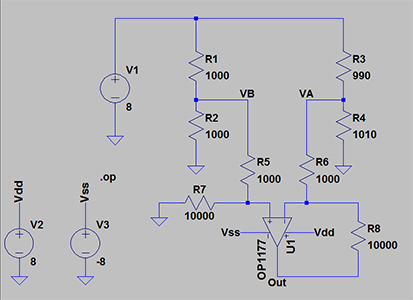
Figure 6
The simulation gives \(v_B=3.82609~V\) and \(v_A=3.85277~V\) that is consistent with our hand calculations. Substituting the value of \(v_A=3.85277~V\) into Equation 3 gives \(R_{in,n}= 10.287~k\Omega\). Although the resistance “seen” at the inverting input is smaller than \(R_{in,p} = 11~k\Omega \), the difference is smaller than that predicted by Equations 1 and 2.
Is This Going to Affect Linearity?
As the final takeaway from this article, I would like to attract your attention to an interesting observation regarding the circuit linearity.
With the bridge shown in Figure 7, the output is given by the following equation:
\[v_{out, Bridge}=v_A-v_B=\frac{\Delta R}{2R_0}V_{DC}\]
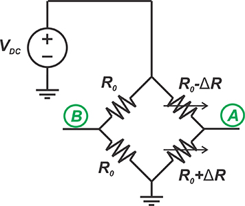
Figure 7
As you can see, the output has a linear relationship with the changes in the sensor resistance value (ΔR).
The discussion of the previous section reveals that the loading effect of the difference amplifier changes with ΔR. Therefore, we can conclude that, while the bridge was originally linear, the overall response of the bridge connected to the difference amplifier is non-linear.
To verify this, we repeat the above LTspice simulations for several different values of ΔR. The result is shown in Figure 8.
In this figure, the blue curve plots the absolute value of the amplifier output (-Vout) against ΔR.
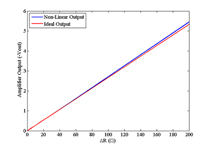
Figure 8
The red curve is the straight line that goes through the points corresponding to ΔR=0 and ΔR=5 Ω.
We can consider this line as the desired linear response (with small values of ΔR, the circuit is expected not to exhibit non-linear behavior). As you can see from the above figure, the actual response gradually deviates from our linear curve.
Note that in many practical applications, ΔR might not vary as much as it does in the above figure. The figure only attempts to show how a voltage-dependent loading effect can lead to non-linearity.
If we assume that the maximum value of ΔR is 10 Ω, we’ll see that the absolute value of the amplifier output (-Vout) and the value given by the linear response are 0.2668 V and 0.2667 V. We can use these values to calculate the percentage end-point linearity error for ΔR=10 Ω as:
\[Percentage~Error=\left (\frac {V_{Non-linear}-V_{Linear}}{V_{Linear}} \right ) \times 100 \% =\frac {0.2668-0.2667}{0.2667} \times 100 \% \approx 0.04 \%\]
Conclusion
The input impedance of an amplifier can have a loading effect on the bridge circuit and affect the accuracy of the measurement system. Even with an infinite CMRR, the unbalanced loading effect of the amplifier allows the common-mode voltage of the bridge circuit to produce an error signal at the output. Therefore, in addition to having high common-mode rejection, in-amps should provide high and equal input impedances.
While a difference amplifier can provide a high CMRR; its input impedances are limited and unequal. This can unbalance the bridge and even degrade the circuit linearity.
To see a complete list of my articles, please visit this page.
Related Content