 Facebook
 Google
 GitHub
 Linkedin
How to Eliminate Reflection Noise in Your Next PCB Design
What is reflection noise? What effects can it have on the functionality of your custom PCB? How can you mitigate it with better design practices?
What is reflection noise? What effects can it have on the functionality of your custom PCB? How can you mitigate it with better design practices?
This article is one in a series inspired by the "Dean of Signal Integrity," Dr. Eric Bogatin's keynote address at Altium Live 2018.
Other articles in the series include:
- What is Inductance and How Does it Apply to Ground Bounce?
- How to Reduce Ground Bounce: Mitigating Noise with PCB Design Best Practices.
- The Path of Least Impedance: How to Use Return Paths for Better PCB Design
This article focuses on reflection noise and how you can reduce it with smart layout choices.
What Is Reflection Noise?
Whenever we send a signal from one digital integrated circuit to another on our PCBs, we change the state of a signal line. That change in state and the accompanying changes in the electromagnetic fields can be described as a wave as it moves through the circuit. Waves are phenomena that transfer energy from one location to another, with conductors guiding the path of propagation.

This is an artistic impression of magnetic energy surrounding a wire as the potential of the wire changes.
Reflection noise results when an electromagnetic wave encounters a boundary from one medium to the next. When the wave meets the boundary, part of the energy is transmitted as signal and part of it is reflected.
![]()
This animation illustrates that, when waves travel from one medium to another, not all energy is transmitted—a portion of the energy is reflected back to its source.
For electrical engineers, the medium where this boundary occurs is usually described in terms of its electrical impedance; that is, the boundary is where impedance changes.
Impedance is composed of resistive and reactive elements. Resistors dissipate a circuit’s energy as heat. The recoverable energy in a circuit exists in the electromagnetic fields that permeate and surround conductors, inductors, and capacitors.
Whenever the impedance changes in a circuit, some amount of reflection will occur. The reflected wave will travel back to the next boundary (the location where there is a change in impedance) and reflect again.

This 1D wave illustration shows a wave pulse reflected between two points. The energy is attenuated over time/distance.
The process will continue indefinitely until the energy is absorbed by the circuit or dissipated into the environment.
Why Is Reflection Noise a Problem?
For signal lines, there will be reflection points at your driver and receiver. The job of the engineer is to minimize the amount of reflected signal and maximize the amount of transmitted signal through impedance matching.
If that is not possible, the additional energy will need to be dissipated before it accumulates and drowns out a signal with noise.
If the energy of the reflected pulse does not dissipate before the next pulse is generated, the energy will accumulate and add in a phenomenon called superposition. Fortunately, signals attenuate as they pass through resistive elements. So a simple series resistor will eliminate most ringing.
Assessing Noise in Digital Signals
Fourier’s theorem teaches that any wave or wave-pulse can be decomposed into a series of sine and/or cosine waves. If you'd like more insight into this concept, I recommend this video on the harmonic analyzer with Bill Hammack of the University of Illinois.
If you have a sufficiently small rise/fall time, a single pulse can hold in it dozens of small-amplitude waves.
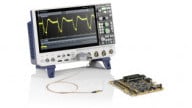
In the image below, you can see an undamped digital signal switching logic states from low to high.

An undamped digital signal (yellow, channel 1) captured on a TI Lightcrafter as it switches logic states from low to high.
Now check out the image below, where the left-hand image shows a composite wave pulse created through the successive superposition of decreasing amplitude odd-harmonics of the original wave. For signals of practical interest, we can decompose the waveform into a series of sine waves.

As the above figures show, a real digital signal has a large bandwidth and any portion of that energy might create a resonance in your circuit. This is in contrast to RF signals that have very narrow bandwidth with easy to calculate resonances.
If you do manage to create standing waves, you will create enormous sources of noise that can overwhelm any signal line in the vicinity.

This gif shows that a wave (orange) reflected at a particular wavelength can combine with its reflection (blue) to create a high amplitude standing wave (green). This phenomenon will happen at odd-integer multiples of ½ wavelength, where the wavelength is twice the length of your trace.
How to Reduce Reflection Noise
There are several methods you can use to manage reflection noise in your design. Here's an overview of some of the techniques at your disposal.
Maintain Constant Impedance
The first thing you should consider is how to maintain constant impedance for your traces whenever possible. Remember: reflections occur when impedance changes.
- Calculate the impedance of your traces
In order to maintain constant impedance, you'll need to be able to calculate the impedance of your traces. Your PCB program should allow you to do this, but there are also online tools available.
Once you determine what your trace and space widths are, maintain them along your routes.
- Consistency across traces
To maintain constant impedance in your differential pairs or single-ended traces, you must maintain constant trace-width, constant spacing, and constant separation from all other conductors. If you route over your impedance-controlled pairs with a random trace, you will change the impedance and create a point of reflection.

-
Use impedance-matching circuitry where impedance changes
When you must change impedance (e.g. from a linear-amplifier to an antenna), use impedance-matching circuitry (calculated with Smith Charts, online tools, etc…).
Reduce Reflection Points
You can also consider how to reduce the occurrence of reflection points in the first place.
- Watch your vias at the edge of the board
Vias can be a problem for high-speed circuit designers. If the via extends beyond the signal traces to unused layers, the impedance of the circuit suddenly changes. At the transition at the edge of a board, there is an impedance mismatch as the traces leave the via (~50-150 ohms) and enter air (~377 ohms). This creates a reflection point at that location that can severely degrade a signal.
- Back-drill your vias
The solution is to have your PCB manufacturer “back-drill” your vias to remove the via from the board on the unused outer layers. Back-drilled vias significantly improve logic transitions.

Image of back-drilled vias from Sanmina-SCI
Mitigate Existing Reflection Noise
- Use damping resistors
Another important technique is to use damping resistors in series near all driving signal sources with fast rise/fall times. This is sometimes referred to as a snubbing resistor.

Any signal reflection that occurs will be quickly attenuated by each pass through the resistor. These are typically <100Ω resistors placed close to the driving signal source (e.g., clock source, GPIO, etc…).
The general idea is to create a damped circuit—where the signal rises to the appropriate logic level once without excessive overshoot and ringing.
Summary
For high-speed signal lines, maintaining constant impedance is critical to designing a working circuit. When moving a signal from one IC to another, include damping resistors to prevent ringing.
If you have additional comments or questions, please share them below!
Related Content


thank you very much for valuable information, is there anyway to show me how to use snubbing resistor in case of using TL494 VCO IC with 12K resistor as RT and 10nF Cap. as CT to reduce Noise!
good article