Facebook
 Google
 GitHub
 Linkedin
How to Optimize the Transient Response of a Phase-Locked Loop
In this article we’ll explore the mathematical relationships that will help you to design a PLL that quickly and smoothly locks onto the input frequency.
In this article we’ll explore the mathematical relationships that will help you to design a PLL that quickly and smoothly locks onto the input frequency.
Supporting Information
- What Exactly Is a Phase-Locked Loop, Anyways?
- How to Simulate a Phase-Locked Loop
- Understanding Phase-Locked Loop Transient Response
If you already have experience and familiarity with phase-locked loops but you’re looking for some theoretical details regarding the design of the loop filter, this article will (hopefully) be just what you need. If you’re interested in loop-filter dynamics but don’t yet have a solid understanding of general PLL functionality, I suggest that you start by reading the articles listed above.
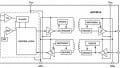
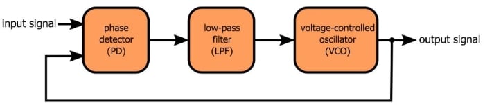
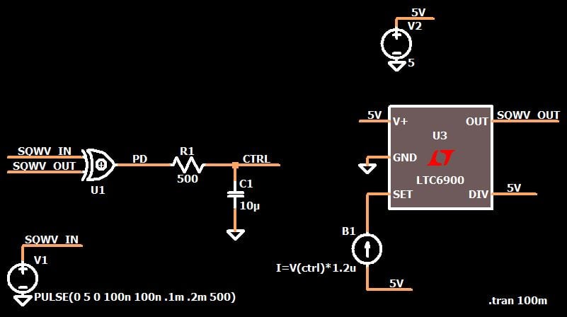
The following diagram conveys the basic structure of a PLL, and below the diagram is the schematic for my LTspice implementation.
This article is about how to design the loop filter for optimal transient response, but as you will see, this design process cannot occur “in isolation,” because the transient response is influenced also by the gain of the phase detector and the gain of the VCO.
Smoothing/Filtering/Averaging
If you’ve read the previous PLL articles, you already know why the system must include a low-pass filter: we need something that transforms the phase detector’s output signal into a slowly varying voltage that can be used to adjust the frequency of a voltage-controlled oscillator. There are different ways to conceptualize this:
- The low-pass filter attenuates the high-frequency components in the PD output signal, such that the low-frequency behavior becomes dominant.
- The PD output signal is equivalent to a PWM waveform, and the filter smooths it into the corresponding analog signal level.
- The filter provides the mathematical functionality of extracting the average value from the PD output.
These are all valid interpretations, and if one makes more sense to you than the others, by all means focus on it. A critical step in understanding (and remembering) is forming images and connections that harmonize with your own cognitive idiosyncrasies.
The Math
Rigorous mathematical analysis of PLL transient behavior is not straightforward. However, we can obtain adequate optimization results by using a fairly simple linear approximation. In this approximation, a transfer function is assigned to each of the three functional blocks. If you combine these into one transfer function that describes the entire PLL, you end up with a second-order expression that can be used to find equations for the PLL’s natural frequency and its damping ratio. It is a second-order (i.e., two-pole) system because the low-pass filter contributes one pole and the VCO contributes one pole; thus, this approximation is valid only with a first-order LPF.
I don’t think you need to worry too much about the mathematical details; the main point is that we can use the damping ratio to help us design the low-pass filter. Here is the equation for a PLL’s damping ratio (usually denoted by ζ, but I’ll use DR):
$$DR=\frac{1}{2}\sqrt{\frac{\omega_{LPF}}{K}}$$
As you can see, there is a fairly straightforward relationship between the damping ratio and the cutoff frequency of the LPF. Two questions arise, though:
- What is K?
- What value should we use for DR?
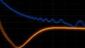
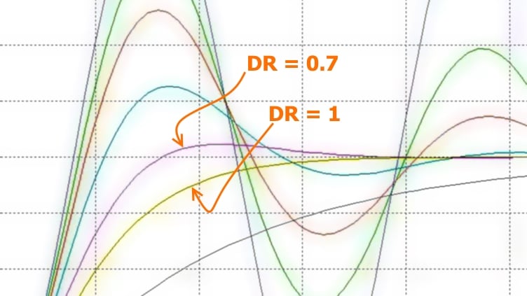
The second question is easier than the first. We’re modeling the PLL as a typical second-order control system, which means that the same damping principles apply: If the DR is too low, the step response will exhibit excessive oscillation. If it’s too high, the system will take a long time to reach the steady-state condition. As shown in the following plot, the ideal DR is around 0.7 (if you want the system a bit underdamped), around 1.0 (if you want the system a bit overdamped), or somewhere in between.
Now all we need is K, which represents the overall gain of the system; it is calculated by multiplying the gain of the phase detector by the gain of the VCO. Unfortunately, this is where things get complicated.
The Frequency/Gain/Cutoff-Frequency Balancing Act
Let’s say you have a phase-detector gain of 1 V/radian (this means that one radian of phase difference between the two inputs will lead to 1 V of output amplitude). Let’s assume also that a 1 V increase in the control voltage increases the VCO frequency by 1000 Hz; since 1000 Hz ≈ 6283 rad/s, our VCO gain is 6283 (rad/s)/V.
$$K=K_{PD}\times K_{VCO}=1\frac{V}{rad}\times6283\frac{rad/s}{V}=6283\ s^{-1}$$
If we want DR = 1, we will have the following equation:
$$1=\frac{1}{2}\sqrt{\frac{\omega_{LPF}}{6283\ s^{-1}}}$$
After a bit of math we end up with ωLPF = 25132 rad/s. Converting back to hertz, we see that the cutoff frequency of the low-pass filter must be 4 kHz. This seems like a perfectly reasonable result, but if you ponder this number for a minute you might start to recognize a problem: What happens if we want to use the PLL with frequencies that are lower than or comparable to the LPF cutoff frequency? The purpose of the low-pass filter is to smooth out the phase-detector waveform, but this will occur only when the filter’s cutoff frequency is significantly lower than the frequencies being generated by the PD.
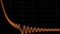
As an example, if I calculate the overall gain of my LTspice PLL and then design the RC filter based on this gain and DR = 1, my control voltage looks like this:
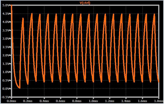
The fundamental problem here is that ωLPF cannot (as I said toward the beginning of the article) be selected in isolation. As you can see in the DR equation shown above, a certain DR requires a certain ratio between ωLPF and K, and ωLPF in turn is restricted by the PLL’s intended frequency range. Thus, transient-response optimization is not simply a matter of finding K and then calculating the LPF’s cutoff frequency. Rather, you have to ensure that the value of K is small enough to allow you to choose a cutoff frequency that is low enough for the PLL’s expected operational environment, and then you can fine-tune the cutoff frequency using the equation that relates DR to ωLPF and K.
Conclusion
This article introduced a bit of math-based PLL analysis in order to explain a procedure for designing a PLL that achieves frequency lock without excessive oscillation or excessive delay. A simple equation allows us to calculate the appropriate LPF cutoff frequency based on the PLL’s overall gain and the desired damping ratio, but the gain must be low enough to allow for a cutoff frequency that provides sufficient attenuation of the high-frequency components in the PD output waveform.
We will continue to explore this topic in the next article.