 Facebook
 Google
 GitHub
 Linkedin
Designing and Simulating an Optimized Phase-Locked Loop
In this article we’ll explore PLL transient-response optimization using simulations and a design example.
In this article we’ll explore PLL transient-response optimization using simulations and a design example.
Supporting Information
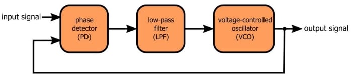
- What Exactly Is a Phase-Locked Loop, Anyways?
- How to Simulate a Phase-Locked Loop
- Understanding Phase-Locked Loop Transient Response
- How to Optimize the Transient Response of a Phase-Locked Loop
Perhaps you’ve noticed that lately I’ve been writing articles about phase-locked loops. A PLL is an interesting system, in my opinion, and I’m glad that we have the opportunity to take a detailed look at this topic.
If you’re not already familiar with PLLs, I recommend that you read at least the first and last articles listed under “Supporting Information,” though in my opinion they’re all worth reading (not a surprising perspective considering that I wrote them). The article entitled “How to Optimize the Transient Response of a Phase-Locked Loop” is particularly important because it provides background information that will help you to understand what we’re doing in this article.
(Very) Brief Recap
A PLL can be modeled as a typical second-order control system, and consequently it is possible to design the PLL such that it has a desirable damping ratio—i.e., such that it quickly and smoothly locks onto the input frequency. The damping ratio (DR, usually denoted by ζ) is related to the LPF cutoff frequency (ωLPF) and the overall gain (K) according to the following equation:
$$DR=\frac{1}{2}\sqrt{\frac{\omega_{LPF}}{K}}$$
We can see from this equation that a chosen DR requires a certain ratio between the cutoff frequency and the gain. Thus, you can’t simply choose a DR and then calculate the cutoff frequency based on K, because this could result in an LPF that doesn’t adequately smooth out the PD signal. Rather, you also have to reduce K until it is small enough to allow for an appropriate cutoff frequency.
The Problem of High Gain
In the previous article I showed you the not-at-all-smooth control signal that my PLL generates when I try to optimize the low-pass filter without adjusting gain. Let’s take a closer look at what I did there.
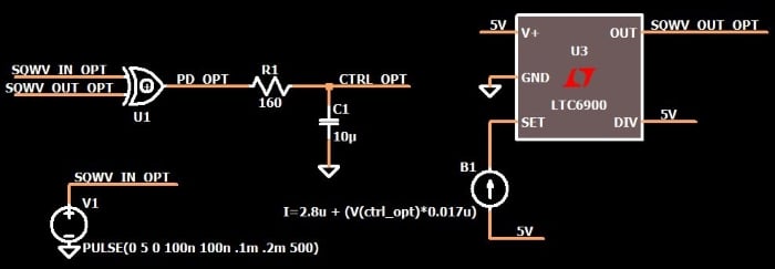
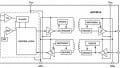
This is the original circuit (i.e., before optimization):
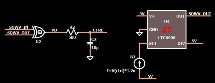
The overall gain of the PLL is the gain of the phase detector multiplied by the gain of the VCO.
$$K=K_{PD}\times K_{VCO}$$
The gain of the PD relates the phase difference between the input signals to the amplitude of the output signal. My phase detector is an XOR gate; if I input two perfectly out-of-phase square waves, the output will always be logic high, which in my circuit means 5 V. “Perfectly out-of-phase” corresponds to a phase difference of π, and therefore my PD gain is (5 V)/(π radians) ≈ 1.6 V/radian.
The gain of the VCO relates the change in control voltage to the change in frequency. If the control voltage in my LTspice circuit increases by 1 V, the control current increases by 1.2 µA. By running a few simulations I determined that a 1.2 µA increase in current corresponds to a ~2.13 kHz increase in frequency. Thus, the gain of my VCO is 2130 Hz/V; however, we need to maintain consistent units, so in the calculation we’ll use (2130 × 2π) ≈ 13,383 (rad/s)/V.
The total gain, then, is
$$K=K_{PD}\times K_{VCO}=1.6\ \frac{V}{radian}\times13383\ \frac{rad/s}{V}\approx21413\ s^{-1}$$
Now let’s calculate the cutoff frequency that we need for DR = 1.
$$1=\frac{1}{2}\sqrt{\frac{\omega_{LPF}}{21413}}\ \ \ \Rightarrow\ \ \ \omega_{LPF}=85652\ \frac{rad}{s}\approx13632\ Hz$$
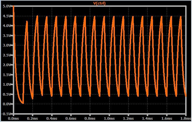
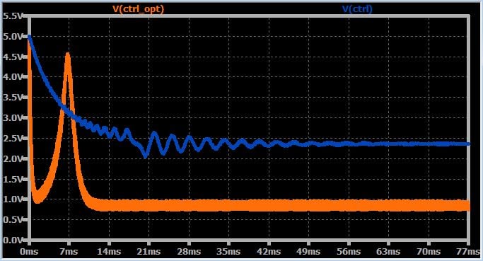
Considering that the PLL’s input signal has a frequency of 5 kHz, it is not surprising that the control signal looks like this:
The Trade-Off
You may have realized by now that the process of PLL optimization involves an irksome trade-off. To suppress high-frequency components in the PD signal we need a low cutoff frequency, and a low cutoff frequency requires a low gain. The problem here is that lower gain makes the PLL compatible with a narrower range of input frequencies:
- The control voltage has a limited range; in my case it is 0 to 5 V.
- The VCO output frequency is proportional to the control voltage.
- A lower VCO gain means that a given control-voltage range maps to a narrower output-frequency range.
- Thus, lowering the gain reduces the range of acceptable input frequencies, because the PLL cannot lock onto a frequency that would require a control voltage that is outside of the circuit’s control-voltage range.
Does This Optimization Thing Really Work?
As far as I can tell, yes. I redesigned my LTspice PLL with transient-response optimization in mind, and the results look good, as you’ll see shortly.
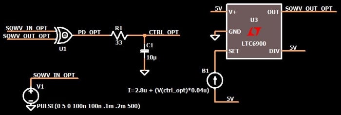
Here’s the procedure:
- As discussed above, my VCO frequency increases by about 2.13 kHz for each 1.2 µA of control current, so the frequency-to-current relationship is 1775 Hz/µA ≈ 11153 (rad/s)/µA.
- I’m expecting input frequencies near 5 kHz, and let’s say that I want an LPF cutoff frequency that is lower by about a factor of ten: ωLPF = 2π × (500 Hz) = 3141.6 rad/s.
- (I’m going to omit units for the gain values so this doesn’t get too cluttered). Using the damping-ratio equation given above with DR = 1 and ωLPF = 3141.6 rad/s, we have K ≈ 785. We divide this by 1.6 (=KPD), and we have KVCO = 490.6. In my simulation I can easily set the VCO gain to whatever I want, but let’s imagine that we are limited to the gain values offered by several off-the-shelf VCOs, the closest of which is 450.
- Now we go back to the DR equation; with DR = 1 and K = 450×1.6 = 720, we find that ωLPF = 2880 rad/s. Converting to hertz, we obtain an LPF cutoff frequency of approximately 485 Hz, and then we change the resistance and/or capacitance accordingly.
- Almost done: Now we need to modify the arbitrary behavioral current source so that the VCO gain is equal to 450. We know that a one-microamp increase in control current will result in a frequency increase of 11153 rad/s, and we also know that we want a one-volt change in control voltage to produce a frequency change of 450 rad/s. Thus, a one-volt change in control voltage must correspond to a 0.04 µA change in current, because 450/11153 = 0.04.
- The last step is to add an offset to the arbitrary behavioral current source. The VCO gain is rather small now, and the offset is chosen such that the initial VCO output frequency is close to the expected input frequency—more specifically, close enough so that our limited control-voltage range is adequate for moving the VCO frequency to the input frequency.
Here is the optimized circuit:
The following plot shows the control voltage for the optimized PLL and the original PLL. That initial spike in the optimized response makes me nervous, but there is no doubt that the optimized control voltage settles on the final value much more quickly than the non-optimized control voltage, and without any oscillation.
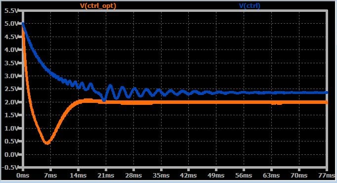
Honestly, though, I don’t really like the new circuit because there is too much ripple in the control voltage. The following circuit is another optimized version but with a lower cutoff frequency (~100 Hz). In this case the damping ratio is 0.91.
Now seriously—did you ever think that PLL transient response could be that good?
Conclusion
We’ve covered additional details regarding the factors that influence a PLL’s ability to lock onto an input frequency rapidly and with minimal oscillation. We went step by step through a design example using an LTspice circuit, and to my great relief the simulation results were consistent with our expectations.
You can click on the orange button to download my LTspice schematic, which includes the optimized circuit and the original one.


This is an excellent description on the PLL dynamic response, Thank you.
From the example optimizations w.r.t. filter’s BW, it seems to me that choice of VCO gain impacts the residual phase shift between input and PLL’s generated output clock signal in steady state. Can you comment on design strategy to minimize the residual phase ?