 Facebook
 Google
 GitHub
 Linkedin
Modeling the Pulse-Width Modulator
Pulse-width modulation can be of many forms. A PWM signal of constant frequency can be obtained by comparing the ramp signal (or carrier signal) with the error between the desired and the actual output voltage signal (Vc, compensator voltage signal).
Pulse-width modulation can be of many forms. A PWM signal of constant frequency can be obtained by comparing the ramp signal (or carrier signal) with the error between the desired and the actual output voltage signal (Vc, compensator voltage signal).
Recommended Level
Beginner
Pulse-Width Waveform Generation and Analysis of Important Parameters in Modelling PWM
Pulse-width modulation can be of many forms. A PWM signal of constant frequency can be obtained by comparing the ramp signal (or carrier signal) with the error between the desired and the actual output voltage signal (VC ,compensator voltage signal).
Mathematically, PWM output is
δ(t) = sign (Vr (t) - VC (t)) [Equation 1]
where:
Vr is the ramp waveform generator output.
VC is the the compensator voltage.
Sign is a sign function which gives the binary output depending upon the difference between Vr and VC.
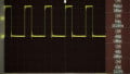
δ(t) have the positive value when ramp voltage Vr is greater than VC , otherwise it is zero as shown in Fig. 2 and Fig. 3.
Vr is the reference or carrier signal which can be a sawtooth, inverted sawtooth and triangular wave. Here, we have considered the sawtooth or ramp signal for the analysis.
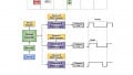
A typical voltage mode control pulse-width modulator block diagram is shown in Fig.1
.png)
Figure 1. Voltage Mode Control PWM Modulator
Peak amplitude of the ramp wave is VP. A comparator compares the output voltage VO and ramp voltage Vr to generate the switching variable δ(t) as shown in Fig. 2 and Fig. 3. There are two cases shown for generating the signal δ(t) depending upon the switching instance at the start or end of the cycle.
.png)
Figure 2. PWM Waveform Generation with Turning-On at the Start of Cycle
From Fig. 2, ramp signal is represented by the equation:
$$V_{r}(t)=V_{cmax} \frac{t}{T}$$
δc can be obtained at the intersection of Vr and VC , thus,
$$V_{r}(δ_{c}T)=V_{cmax}\frac{δ_{c}T}{T}=V_{C}$$
$$\Rightarrow δ_{c}=\frac{V_{C}}{V_{cmax}}$$ where c = 0, 1, 2,….. n [Equation 2]
Therefore, the gain of the compensator is $$G_{C} = \frac{δ_{c}}{V_{C}}=\frac{1}{V_{cmax}}.$$
.png)
Figure 3. PWM Waveform Generation with Turning-Off at the End of Cycle
From Fig. 3, we need to find out the value of switching angle i.e. αc where c = 0, 1, 2…..n.
Here, ramp signal can be expressed as:
$$V_{r}(t)=V_{cmax}-2\,V_{cmax}\frac{wt}{π}$$
And error signal as:
$$V_{C}(t)=V_{cmax}-2\,V_{cmax}\frac{α_{c}}{π}$$
At the intersection point, VC = Vr
$$α_{c}=\frac{π}{2}(1-\frac{V_{C}}{V_{cmax}})$$ [Equation 3]
Thus, the gain of the compensator is $$G_{C}=\frac{d\,α_{c}}{d\,V_{C}}=-\frac{π}{2\,V_{cmax}}.$$
After turning on and off any variation in the compensator signal VC(t), the duty cycle δ(t) will be affected after some delay. Let us say that the value of this delay is T/2.
Then the control transfer function can be expressed as,
$$\frac{δ_{c}(t)}{v_{c}(t)}=G_{c}{e}^{-\frac{sT}{2}}=\frac{G_{C}}{1+\frac{sT}{2}+\frac{{s}^{2}}{2!}{(\frac{T}{2})}^{2}+…}≈\frac{G_{C}}{1+\frac{sT}{2}}$$
Clearly, this pole occurs at the frequency which is double of the switching frequency. As the location for frequency of the state-space average models is near about one decade of the switching frequency, compensator pole can be neglected.
For DC-to-DC converter, PWM reference signal (Vr) is of constant value and independent of modulation technique employed for the steady state. For the dynamic purpose, the reference signal can be considered to be the sum DC value corresponding to the steady state and a sinusoidal signal signifying the small signal perturbation.
Mathematically, it can be written in general as,
$$V_{r}(t)=V_{ro}+V_{r1}\,cos(2π\,f_{1}t\,+\,∅_{1})$$
where f1 is the frequency of the reference signal.
Previously, LTI model that characterizes the small signal behavior of a converter is required for analysis and controller design. This model can be developed for both constant frequency and variable frequency pulse-width modulation. Here, we are going with the constant PWM.
Average duty ratio, $$d\,=\,\frac{V_{ro}}{V_{cmax}}$$
and
Modulation Index, $$M\,=\,2\frac{V_{r1}}{V_{cmax}}$$
The amplitude of the perturbation $$=\frac{V_{r1}}{V_{cmax}}=\frac{M}{2}$$
An example of buck converter is shown in Figure 4. If we alter the duty ratio slowly as compared to the switching frequency, we will get a waveform whose average values change with time. Thus, we need to do averaging for this case. The averaging time must be greater than the switching time but less than the rate of change of the duty cycle.
The duty ratio is altered to get a load voltage having a DC component and a sinusoidal frequency, wa, whose value is lesser than the switching frequency.
The modulated d(t) in that case can be represented as,
$$d(t)=0.5\,+\,0.25\,sinw_{a}t$$
.png)
Figure 4. Buck Converter with Modulated Duty Ratio
As we have studied earlier in the cases of buck, boost and buck-boost converters, either switch or diode conducts at a particular time in continuous conduction mode; and expressed as
$$\dot{x}=[A_{01}δ(t)+A_{02}(1-(δ(t))]x\,+\,[B_{01}δ(t)+B_{02}(1-δ(t))]u$$
But this model is not acceptable to design linear control systems as it has a time-varying function δ(t) which is multiplied by the state variables. Thus, we have to deal with this time-varying problem with averaging. The state-space averaging model obtained over a switching cycle will be
$$\dot{\overline{x}}=[A_{01}d+A_{02}(1-d)]\overline{x}+[B_{01}d+B_{02}(1-d)]\overline{u}$$
Similar equation can be written for the output signal. Here, d is the algebraic average of the duty cycle ratio over a complete cycle.
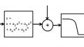
Consider that there is a small disturbance in the controller compensator signal due to variation in the output and the result in the duty cycle is shown by the block diagram below.
We now have,
$$V_{C}(t)=V_{C}+{\check{v}}_{c}(t)$$ and $$d(t)=D\,+\,\check{d}(t)$$
.png)
Figure 5. Block Diagram of the PWM for the Perturbation Case
From Equation 2, we have the following PWM equation for the linear ramp signal:
$$δ_{c}=d=\frac{V_{C}}{V_{cmax}}$$ for 0 ≤ VC (t) ≤ Vcmax
It is clear from this equation that δc(t) is linearly dependent on the VC.
Including the small signal, the final PWM equation is,
$$D+d(t)=\frac{V_{C}+{\check{v}}_{c}(t)}{V_{cmax}}$$
If we separate the steady-state relation and the small-signal relation, we get the following results:
$$D=\frac{V_{C}}{V_{cmax}}$$ and $$\check{d}(t)=\frac{\check{v_{c}}(t)}{V_{cmax}}$$
In Fig. 5, the input signal is continuous while the output has discrete values. Thus, a sampler with sampling rate equal to the switching frequency is needed as shown in Fig. 6.
.png)
Figure 6. PWM Modulator
This model is valid for continuous conduction mode. In the case of discontinuous conduction, we have to consider the three intervals of switching to form the final model.
In the case of the voltage control methodology for the small-scale linear model, the ratio of the duty ratio to the output voltage will be in the second order. Crossover frequency for the voltage control loop must be lower than the resonant frequency to ensure the stability of the system. Also, there exist a right-half plane zero in this transfer function even at frequencies that are less than the resonant frequency. Thus, this model is accurate only for frequencies much lower than fs / 2 (Nyquist rate). This issue can be solved by the adding a current-loop control.


Hi,
I wish to know about the function of the sampler here.
Thanks in advance,
Salil