 Facebook
 Google
 GitHub
 Linkedin
Understanding Verilog Shift Registers
This article will discuss how to implement a shift register in Verilog. The register described can be synthesized and downloaded to an FPGA for test in actual hardware.
This article will discuss how to implement a shift register in Verilog. The register described can be synthesized and downloaded to an FPGA for test in actual hardware.
Verilog Shift Register Basic Concepts/Characteristics
In its simplest form, a shift register consists of a number of storage elements (e.g., flip flops) connected in series, so that the output of one storage element feeds into the input of the next. The storage elements are controlled by a common clock signal:
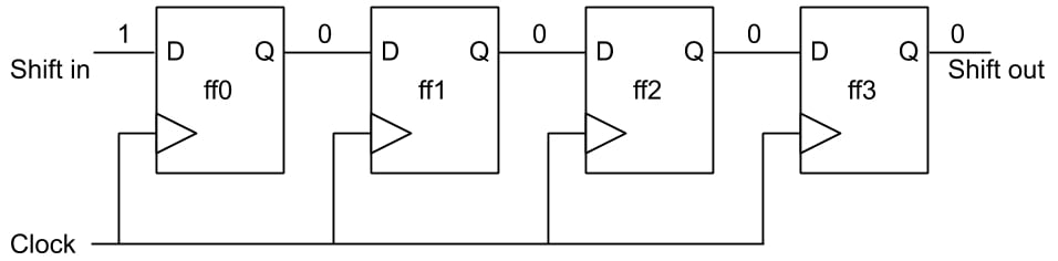
Figure 1. 4-bit shift register
Let’s say we are using positive edge-triggered flip flops. Consider the flip flops labeled 0 and 1 in Figure 1 (ff0 and ff1). The input to ff0 is the input to the shift register. The input to ff1 is the output of ff0, which is also the current value of ff0. On a positive clock edge, ff0 will capture its input and ff1 will capture the current value of ff0.
If all the flip flops start out reset to 0 and we hold the input of the shift register at 1, then a positive clock edge will cause ff0 to capture a 1.
On the second positive clock edge, ff1 will capture a 1 because it has sampled the output of ff0 (see Figure 2):

Figure 2. Result of two positive clock edges or "shifts"
On each successive positive clock edge, the 1 will “shift” to the next flip flop in the chain until it appears at the output of the shift register, which is the output of ff3 in the 4-bit shift register shown above. If we have held the input at 1 during this time, the register will now hold all 1s.
Verilog Shift Register Code
Verilog is a hardware description language, or HDL, which means it can be used to describe actual logic circuit hardware. Because of this, there are several aspects of Verilog that are different from typical software programming languages.
There are two important things to keep in mind when writing Verilog code:
- Just like in an actual circuit, some parts of Verilog code execute simultaneously, not sequentially or line-by-line as in a single-threaded software program.
- Not all Verilog constructs can be synthesized, or turned into an actual logic circuit.
We’ll aim to write synthesizable code in this example. This will also allow us to download our code into an FPGA to actually see it in action!
Module Declaration
We’ll start with a module declaration:
module shiftReg4( input shift_in, input clock, output shift_out );Modules form the basic building blocks of a Verilog-based design. With our shift register declared in a module, we can instantiate as many copies of it as we wish, connected how we like in a larger circuit.
The input and output statements are port declarations—they determine what connections will be available when we instantiate our shift register. For now, we just have a shift input, a clock input, and a shift output.
Reg
Next, we need to define the circuitry and wired connections for our shift register. Like the diagram above, we’ll use four flip flops for this 4-bit shift register.
We can create a flip flop using the reg keyword:
reg bit0; reg bit1; reg bit2; reg bit3; assign shift_out = bit3;Here we have four flip flops named bit0 through bit3.
The bit0 flip flop will have its input connected to the shift_in port; we’ll take care of that in the next block of code.
The bit3 flip flop will have its output connected to the shift_out port, and we have accomplished this with an assign statement, which can be used for wiring and combinational logic.
Procedural Block
Now, we need to tell Verilog what to do with these flip flops, and this is accomplished in a procedural block.
A procedural block can be used to define either combinational or sequential logic but, in this example, we’ll only use one for sequential logic (logic with stored values, e.g., in flip flops).
always @(posedge clock) begin bit3 <= bit2; bit2 <= bit1; bit1 <= bit0; bit0 <= shift_in; end endmoduleThe procedural block starts with the always keyword, followed by a sensitivity list. The sensitivity list tells Verilog when to evaluate the statements in the block; in this case, we evaluate the block on every positive clock edge (@posedge clock).
When the block is triggered on a positive clock edge, we simply shift the contents of each flip flop to the next flip flop in the chain. So, bit3 gets what was previously in bit2, bit2 gets what was in bit1, and so on. Note that we delineate where the block starts and finishes with begin and end statements.
Endmodule
Finally, we end our module with an endmodule statement. Congratulations—you’ve just created a 4-bit Verilog shift register!
Practical Considerations: Indexing and the Shift Operator
We created our Verilog code to match exactly the circuit we envisioned, with four separate flip flops connected in series. This is great for knowing exactly what will be synthesized, but it becomes tedious if we have to manually declare every flip flop in our design.
Luckily, Verilog has many different shortcuts, and here we can use indexing and the shift operator:
reg [3:0] bits; assign shift_out = bits[3]; always @(posedge clock) begin bits <= bits << 1; bits[0] <= shift_in; endThis is much more compact! We’ve declared a 4-bit register all at once with the bracket notation “[3:0],” which indicates that bit 3 is the most significant bit (MSB).
Note that we have to change our assign statement to wire bit 3 of the register to our shift_out signal. Now, instead of writing procedural block statements to individually change each bit, we can use a single statement with the shift left operator (<<) to accomplish what we want. On each positive clock, the data in our 4-bit register will be shifted one position to the left, and the new MSB will be driven on shift_out.
Note, too, that this implementation makes it easy to change the shift order. Currently, we are shifting from LSB to MSB, but we can easily change this so that we’re shifting from MSB to LSB. Try this on your own for practice!
Synthesis in Verilog
One caveat: In Verilog, just declaring a node as reg doesn’t automatically create a flip flop. This is where the principle of synthesis and synthesizable code comes in.
A reg node will hold its value until it is assigned another value. When the code is synthesized to create actual hardware structures, this could result in a flip flop (typically what is wanted), a latch (typically not wanted), or an error, depending on how the node is assigned. Putting “@posedge clock” in our sensitivity list and being careful to always assign to all reg signals in the procedural block ensures that we will get the flip flops we expect.
Uses/Applications
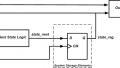
Shift registers often find application in situations where we need to convert from parallel data (typically used internally in a microprocessor or other ASIC) to serial data (often used for communication between components on a PCB or between two separate PCBs). For this purpose, we typically add a load signal and wires to each of the individual flip flop inputs in the shift register so that parallel data can be loaded into the shift register all at once and then shifted out bit by bit.
To implement serial communication protocols such as I2C and SPI, we can use a state machine to control when the individual data bits are shifted out of the register in order to meet the requirements of the scheme we have chosen.
We can also add wires to the outputs of each individual flip flop so that a device can receive serial data bit by bit and then read it out of the shift register in parallel when all bits have been shifted in.
Conclusion
In this article, we discussed how to implement a basic shift register in Verilog. A typical workflow would next involve writing a testbench to instantiate our new shift register and drive some inputs to it so we can verify the correct operation in simulation, before synthesizing the code and downloading it to an FPGA for test in actual hardware.
I hope you enjoyed this short example!


The reg keyword in Verilog simply indicates that the value will be assigned within an always block. You can create combinatorial logic inside an always block—in fact this is very useful for complex combinatorial structures that you may not want to try to define on a single line using an assign statement. The outputs of the always block are still defined as reg even through no register or latch is produced in synthesis. This was actually a rather confusing nomenclature in Verilog (reg != register); consequently SystemVerilog has replaced both regs and wires with the logic keyword.