 Facebook
 Google
 GitHub
 Linkedin
Using QSPICE to Understand and Tune an LED Blinker Circuit
In this article, we examine the oscillation behavior of an LED blinker circuit in QSPICE and learn how to control its ON-time and pulse repetition frequency.
This article is Part 4 of a four-part series on QSPICE for LTspice users. Here’s a quick recap of the series up to this point:
- Part 1: We created and simulated a two-transistor LED blinker circuit in LTspice.
- Part 2: We went through the (somewhat laborious) process of creating a QSPICE schematic from the LTspice circuit.
- Part 3: We imported an LED model from LTspice, then used QSPICE’s waveform viewer to compare its behavior with that of the LED implementation from Part 2.
If you haven’t yet read these articles, you’ll probably want to scan through them before proceeding. Otherwise, let’s pick up where we left off and conclude our investigation of the QSPICE blinker circuit. QSPICE’s waveform viewer will help us see why the circuit works and how we can adjust pulse width and oscillation frequency.
As I alluded to in the series recap, “QSPICE blinker circuit” could actually refer to either of two different schematics. This came about because the LTspice LED component didn’t have a direct equivalent in the QSPICE library. The two schematics represent two different ways of fixing that problem:
- Replacing the LED with a component—in this case, a normal diode in series with a voltage supply—that mimics its current-voltage behavior.
- Manually importing the SPICE model for the LED into QSPICE.
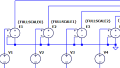
We’ll be using the imported-SPICE-model version of the circuit (Figure 1).
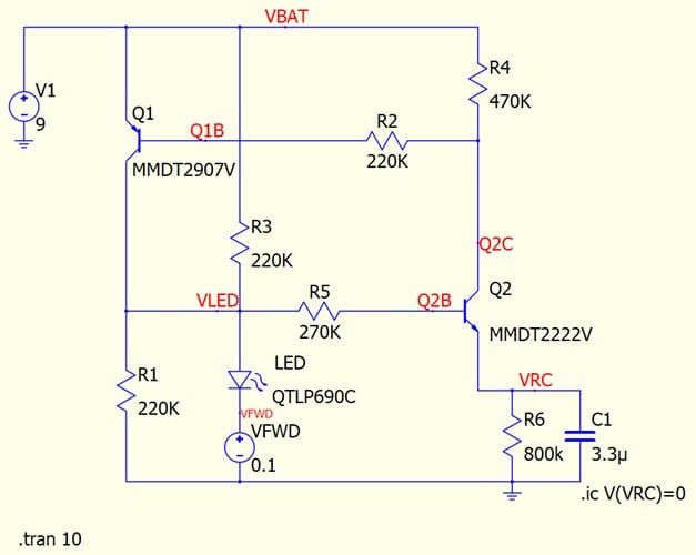
Figure 1. The QSPICE LED blinker circuit we’ll examine in this article.
We learned in the previous article that the imported-SPICE-model version of the circuit will oscillate only if we give it a little extra voltage on the LED node. That’s why we added the VFWD source you see in the figure above—when combined with the QTLP690C LED model, it creates an LED with a slightly higher forward voltage.
As we’ll see in the next section, playing around with VFWD also reveals an important aspect of the blinker circuit’s illumination behavior.
How Forward Voltage Affects Oscillation Frequency
Figures 2 through 4 plot the LED current for three different values of VFWD. We have 100 mV of forward voltage in Figure 2, 400 mV in Figure 3, and 800 mV in Figure 4.
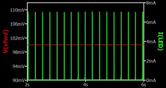
Figure 2. LED blinker circuit with 100 mV forward voltage added.
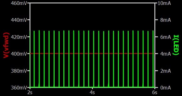
Figure 3. LED blinker circuit with 400 mV forward voltage added.
Figure 4. LED blinker circuit with 800 mV forward voltage added.
Looking at these plots side by side, it’s clear that the pulse frequency is increasing along with the forward voltage. This is important for practical reasons—because different LEDs have different forward voltage characteristics, it means that the oscillation frequency in a real-world circuit is dependent on the specific LED part chosen. It also leads us to some fundamental observations about how the blinker functions.
Understanding the Oscillation Behavior
Node VLED is actually rather complex, being directly connected to the LED, three resistors, and the collector of Q1. The voltage at this node strongly influences the oscillation frequency.
A quick look at the Q2B node in Figure 1 shows us that higher VLED voltage corresponds to higher Q2 base voltage. This suggests that the value of VLED influences Q2’s operation in a way that directly modifies the circuit’s oscillation. Figure 5 shows the relationship between the LED current (green trace) and the voltage at Q2’s collector (red trace).
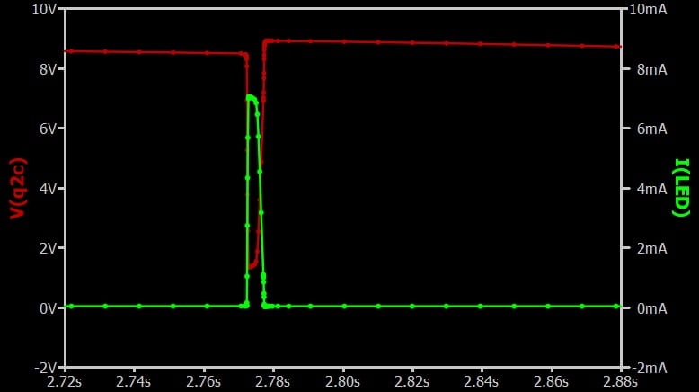
Figure 5. Voltage behavior of Q2’s collector when current flows through the LED.
The above figure shows a major drop in collector voltage when the LED is illuminated. This tells us that when the LED is conducting, higher Q2 base voltage causes Q2 to conduct as well. When Q2 is conducting, its collector voltage is lower.
Q1’s base is connected to the Q2 collector node through R2, so its base voltage decreases as well. As we see in Figure 6, the drop in the Q1 base voltage increases the current flowing through Q1.
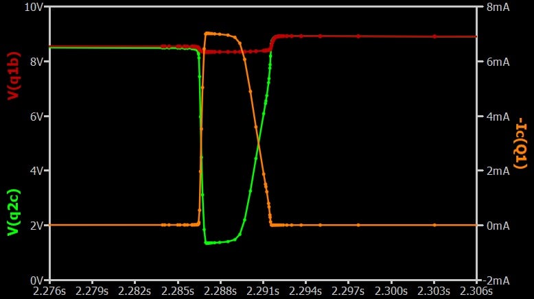
Figure 6. Q1’s base voltage drops in response to a decrease in Q2’s collector voltage, causing the current through Q1 to increase.
We’ve now come full circle—current flowing through Q1 is delivered to the LED. We can summarize the interaction between the LED, Q1, and Q2 as follows:
- Current for LED illumination flows from the power supply through Q1.
- When the LED is conducting, the voltage at the VLED node is higher, and this voltage is influenced by the forward voltage characteristics of the LED.
- When VLED increases, Q2 conducts more current.
- Increasing Q2 current reduces the base voltage of Q1.
Analyzing and Adjusting Oscillation Characteristics
Next, let’s take a look at how the RC network (R6 and C1) can be used to tune the blinker circuit’s frequency and pulse width. We’ll start by examining Figure 7, which plots current through the LED and current delivered to the RC network over the same period of time.
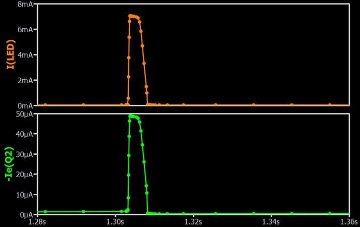
Figure 7. The current flow through the LED and transistor Q2 follow the same pattern.
We can see that the current delivered to the RC network coincides with the current through the LED, and therefore with Q2’s current as well.
As we observe in Figure 8, the current that flows from Q2’s emitter charges up the capacitor (C1), thus raising the voltage across the RC network (VRC). This current is the key to the circuit’s oscillatory behavior.
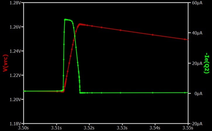
Figure 8. The current through Q2 charges up the RC network.
Q2’s base-to-emitter voltage steadily decreases as VRC increases. When VRC reaches a certain threshold, Q2 stops conducting. This is what causes the behavior of the red trace in Figure 8. Its steep upward slope represents the charging phase, after which the capacitor slowly discharges through R6.
It’s now apparent that the charging/discharging behavior of the RC network is the basis of the circuit’s oscillatory timing. The LED’s ON-time corresponds to the RC network’s charging duration; the delay from the end of one pulse to the beginning of the next pulse is the RC network’s discharge duration. This is illustrated in Figure 9.
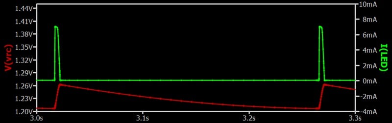
Figure 9. A full cycle of the LED blinker showing the charging and discharging of the RC network.
Adjusting the Frequency
Based on the above, we should be able to increase the frequency by decreasing the value of R6 so that discharge occurs more quickly. Figure 10 tests this by decreasing R6 from 800 kΩ to 400 kΩ.
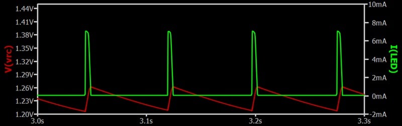
Figure 10. Pulse frequency with R6 = 400 kΩ.
As expected, lowering the resistance resulted in a higher pulse frequency.
Adjusting the Pulse Width
A higher capacitance means that the voltage rises more slowly during the charging phase, so we should be able to widen the pulse by increasing the value of C1. To test that, the plot in Figure 11 was generated with C1 = 10 μF instead of the original 3.3 μF. The value of R6 is unchanged from Figure 10, and the same horizontal axis limits are used so that the pulse widths can be directly compared.
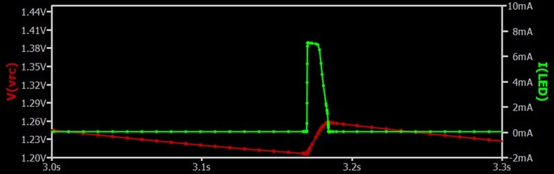
Figure 11. Pulse width for C1 = 10 μF, an increase of 6.7 μF from Figure 10.
As you can see, the new pulse is significantly wider. With relatively simple changes to the RC network, we can control both the pulse repetition rate and the pulse width for the LED blinker.
Wrapping Up
This concludes my series on QSPICE for LTspice users. My purpose in writing this series was twofold:
- To help SPICE users understand and optimize the task of moving LTspice circuits into QSPICE.
- To provide a moderately detailed and hands-on introduction to drawing schematics, performing simulations, and analyzing results with QSPICE.
If you've used QSPICE and have any further observations or handy tips to share, please feel free to leave us a note in the comments!
This article is Part 4 of a series on QSPICE for LTspice users. Links to Parts 1 through 3 can be found in the article introduction. A complete list of articles in this series is also included below:
- Introduction to QSPICE for LTspice Users
- Transferring LTspice Schematics to QSPICE
- Transferring SPICE Models from LTspice to QSPICE
- Using QSPICE to Understand and Tune an LED Blinker Circuit
All images used courtesy of Robert Keim
Related Content


Such a pity that you didn’t build the circuit to see how the simulations compared with reality.