Facebook
 Google
 GitHub
 Linkedin
Using Single-Ended Amplifiers in Low-Side Current Sensing: Error Sources and Layout Tips
Learn how to use single-ended amplifiers in low-side current sensing, including PCB layout tips and considerations, as well as a layout example based on an op-amp in the SOT23 package.
In the first part of this article, we discussed that the non-inverting configuration of a general-purpose op-amp can be used in low-side current sensing. Inspired by the article “How to lay out a PCB for high-performance, low-side current-sensing designs” from TI, this article attempts to further clarify the sources of error that can affect our measurement when using single-ended amplifiers in low-side current sensing.
Using Single-Ended Amplifiers in Low-Side Current Sensing
The main advantage of low-side sensing is that relatively simple configurations can be used to amplify the voltage across the shunt resistor. For example, the non-inverting configuration of a general-purpose op-amp can be an effective option in cost-sensitive motor control applications that need to be able to compete in the consumer market space.
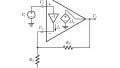
The circuit diagram based on the non-inverting configuration is shown in Figure 1.
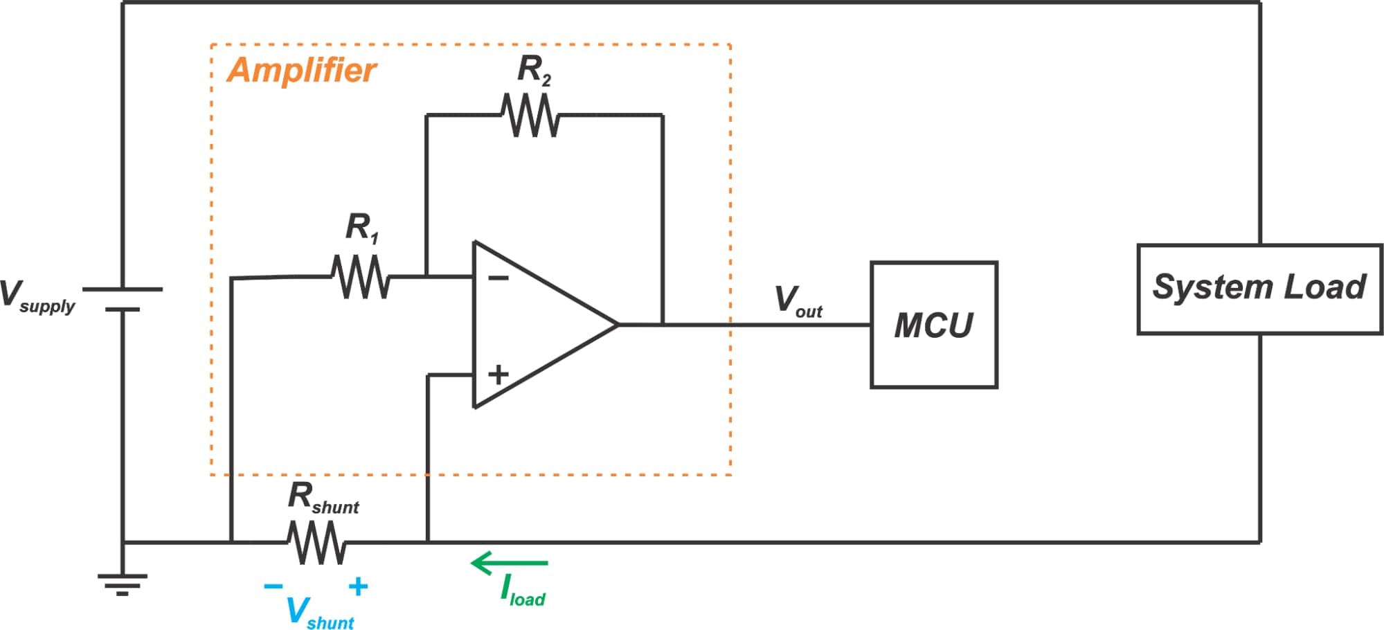
Figure 1.
However, this low-cost solution can be affected by several different sources of error. To make an accurate measurement of current, we need to take into account any non-ideal effect that can affect the susceptible nodes of the circuit such as the amplifier inputs. We’ll discuss this in greater detail below.
Trace Resistance
One important source of error is the parasitic resistance from PCB traces that appear in series with Rshunt. Since Rshunt has a small value in the range of milliohms, any parasitic resistance in series with Rshunt can lead to a significant error. Modeling this parasitic resistance by Rstray, we obtain the schematic in Figure 2.
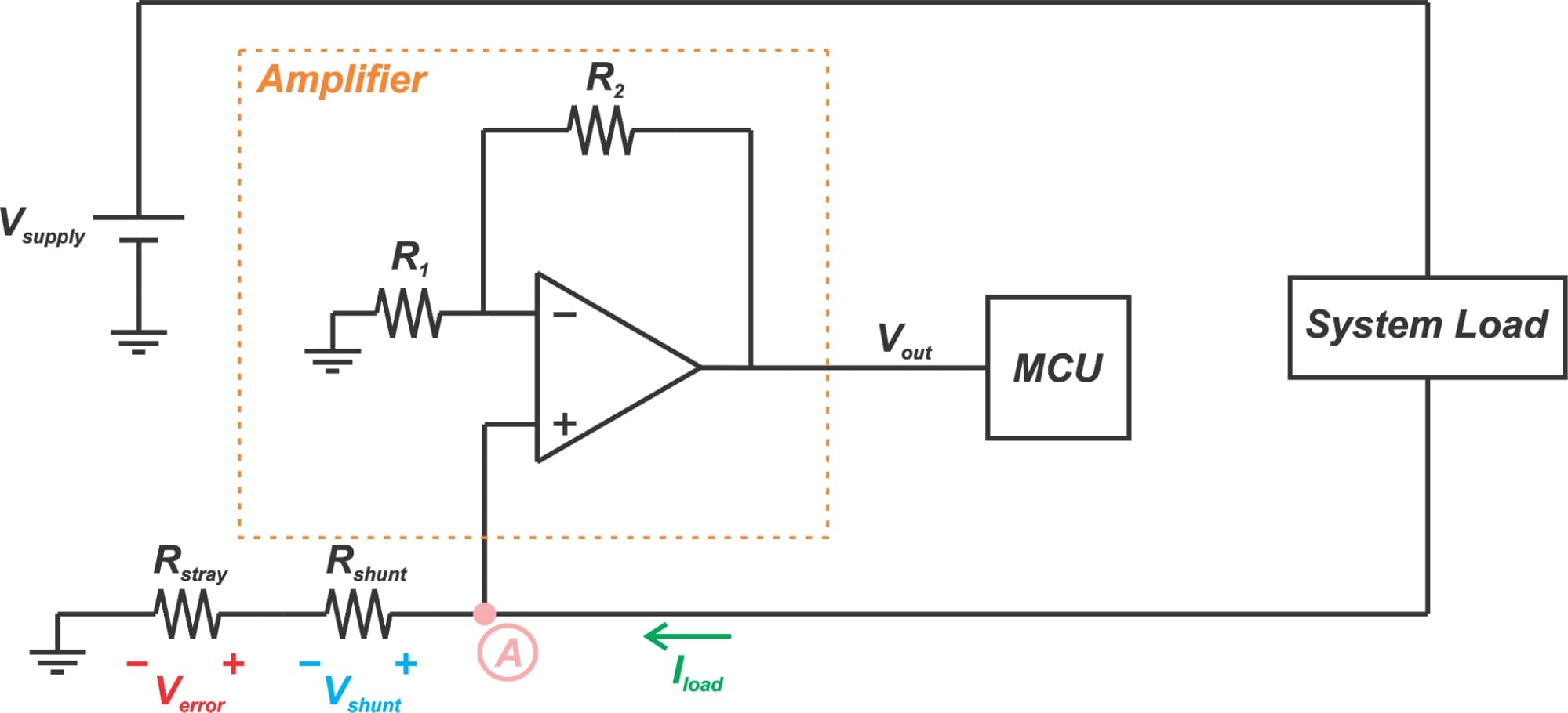
Figure 2.
Depending on the application, Iload can be as high as hundreds of amperes. As a result, even a small value of Rstray can produce a considerable error voltage Verror. This error voltage will be amplified by the gain of the amplifier and appear at the output.
Since the temperature coefficient of copper resistance is fairly high (about 0.4%/°C), the value of Rstray and consequently, the error voltage can widely vary with temperature. Hence, the stray resistance can create a temperature-dependent error in systems that undergo wide temperature variations. To reduce the error voltage Verror, we should avoid long traces to minimize Rstray.
It is worthwhile to mention that a more efficient solution to eliminate the error from Rstray is to use a different amplifier rather than a non-inverting configuration. As you can see from Figure 2, a non-inverting configuration has a single-ended input. It senses the voltage at node A with respect to ground. However, a difference amplifier has a differential input and senses the voltage across Rshunt. This is shown in Figure 3.
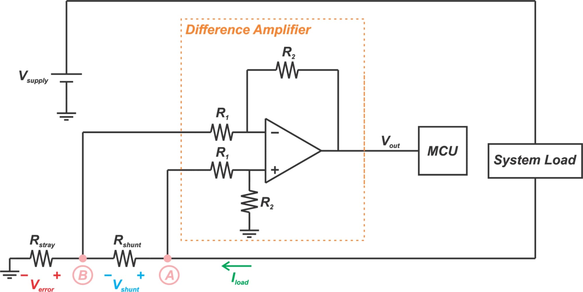
Figure 3.
The transfer function of a difference amplifier is given by:
\[v_{out}=\frac{R_{2}}{R_{1}}\left(v_{A}-v_{B}\right)=\frac{R_{2}}{R_{1}}V_{shunt}\]
Since the differential input of the amplifier senses the voltage across the shunt resistor, the resistance from the PCB trace cannot produce an error. We’ll examine the difference amplifier configuration in greater detail in a future article.
Solder Resistance
Another source of error is the solder resistance that appears in series with the sense resistor. This is illustrated in Figure 4.
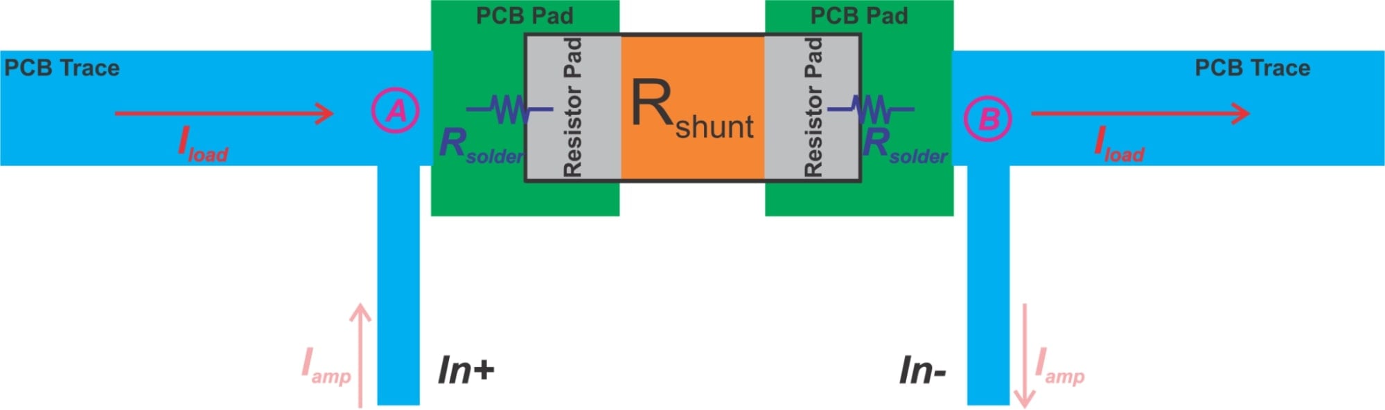
Figure 4.
In this figure, the load current flows from left to right in the direction of the red arrow. The vertical traces connect the shunt resistor to the amplifier inputs (In+ and In-). Hence, the amplifier senses the voltage difference between points A and B. The actual value of the sense resistor will be Rshunt+2Rsolder. The solder resistance can be in the range of a few hundred micro-ohms.
The error becomes significant especially when a small shunt resistor is employed. For example, with a 0.5 mΩ shunt resistor and Iload=20 A, the error from solder resistance can be as large as 22%. To combat this problem, the amplifier inputs should be connected directly to the shunt resistor rather than the current-carrying traces. Figure 5 shows an example layout that can give a more accurate result.
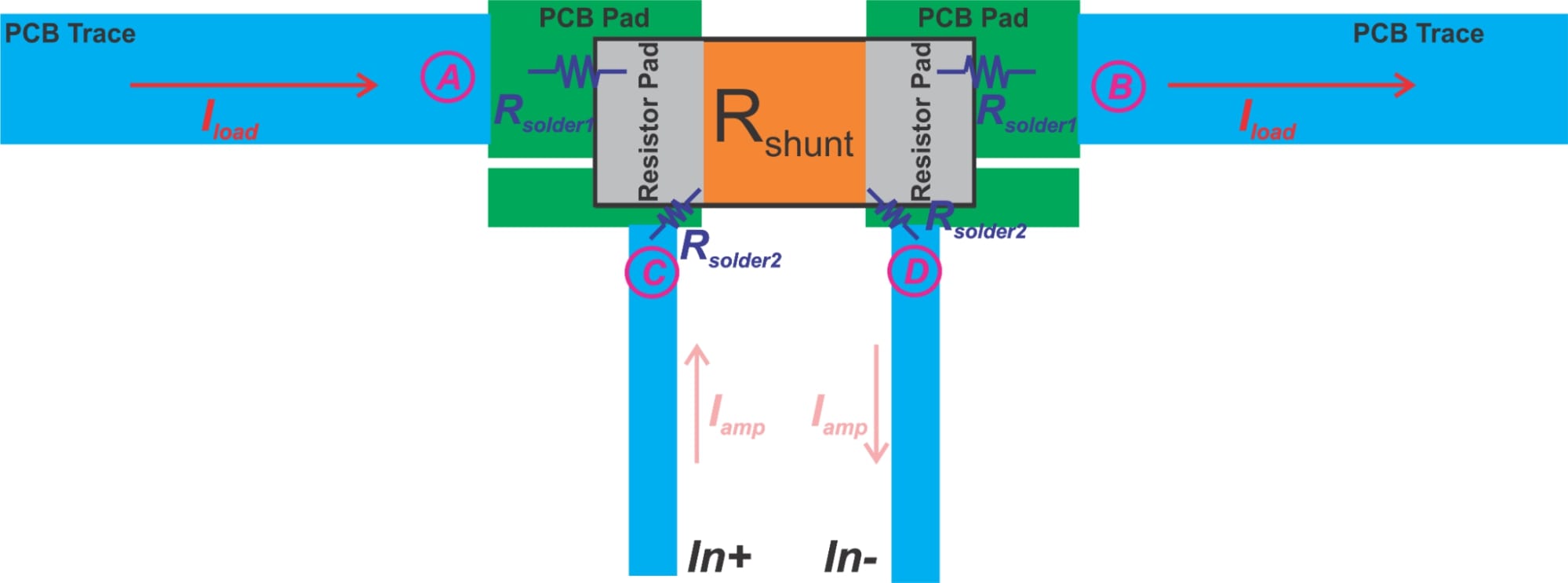
Figure 5.
In this case, there are two pairs of PCB pads: one pair is used to connect Rshunt to the load and the other pair is used to connect Rshunt to the amplifier inputs. In high-current applications, the current drawn by the amplifier (Iamp) is much much less than Iload. That’s why the above layout can reduce the error from solder resistance.
To better understand this technique, let’s compare the sensed voltage in both cases. With the layout shown in Figure 4, the sensed voltage is:
\[v_{A}-v_{B}=\left(R_{shunt}+2R_{solder1}\right)\times \left(I_{load}+I_{amp}\right)\]
Since Iamp is much much smaller than Iload, we have:
\[v_{A}-v_{B}\approx\left(R_{shunt}+2R_{solder1}\right)\times I_{load}=R_{shunt}I_{load}+2R_{solder1}I_{load}\]
Equation 1.
This gives an error voltage of 2Rsolder1Iload. What about the layout in Figure 5? The circuit diagram of this layout is shown below:
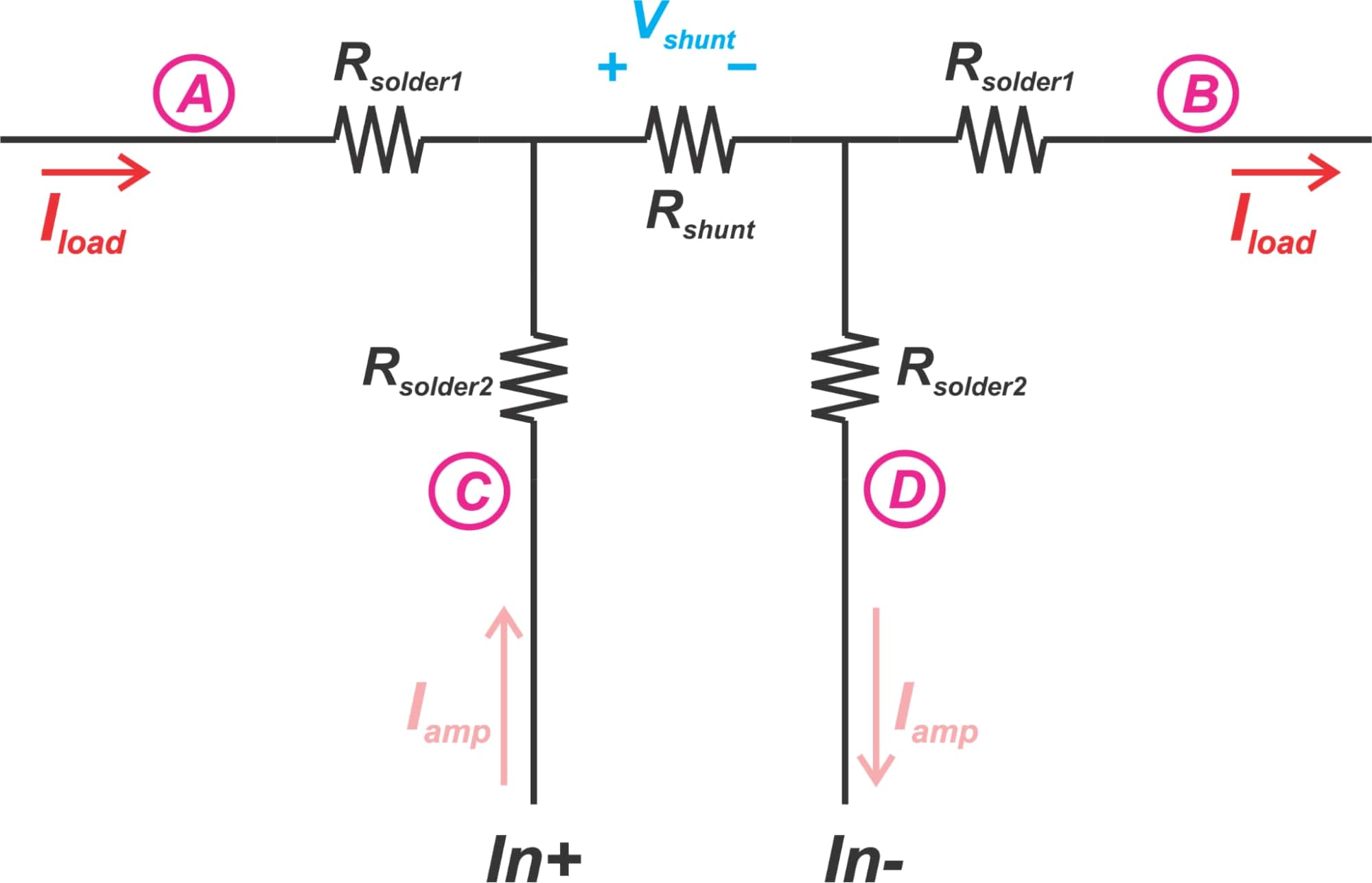
Figure 6.
Note that the current Iload returns to its source without going through Rsolder2. The measured voltage is:
\[v_{C}-v_{D}=R_{shunt}\times\left(I_{load}+I_{amp}\right)+2R_{solder2}I_{amp}\approx R_{shunt}I_{load}+R_{solder2}I_{amp}\]
In this case, the error is 2Rsolder2Iamp which is much less than that of Equation 1 because Iamp is much much less than Iload. This technique is commonly referred to as Kelvin sensing and finds use in many application areas. It allows us to make accurate measurements of impedance. Some of the other PCB layouts that employ the Kelvin sensing technique are shown in Figure 7.
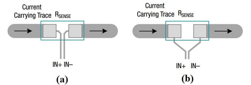
Figure 7. Image (adapted) courtesy of TI.
You can find more complicated layout examples for Kelvin connection in “optimize high-current sensing accuracy by improving pad layout of low-value shunt resistors” from Analog Devices.
You might wonder which one of the three layouts depicted in Figures 5 and 7 can lead to a more accurate measurement? It should be noted that it is difficult to answer this question because the result depends on the resistor that you employ in your design. Different resistor manufacturers might use different measurement locations when reporting the nominal value of the resistor.
For example, if the resistor manufacturer has measured the resistor on the inside the pads, then the layout in Figure 7(a) can give us more accurate measurements.
Noisy Ground
Figure 8 shows another source of error: noisy ground.
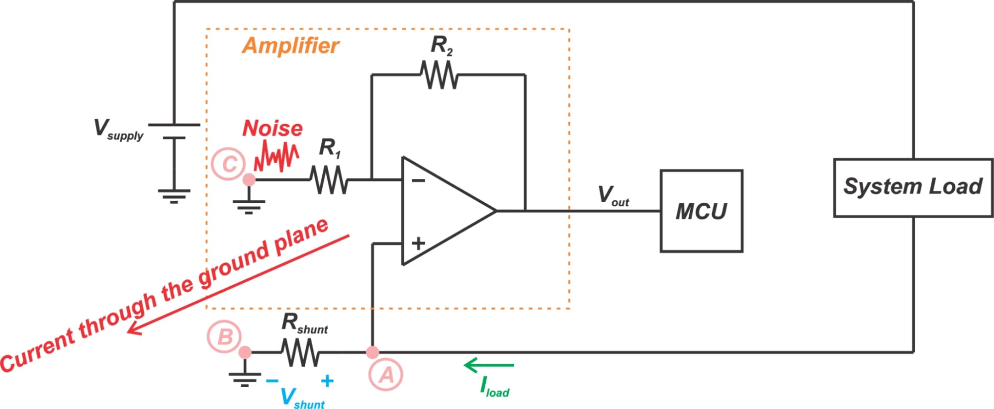
Figure 8.
We discussed that since the non-inverting configuration has a single-ended input, it measures the voltage at node A with respect to ground. Assume that our board has a dedicated ground plane. We can place a via very close to Rshunt to keep point B at the system ground potential and minimize the error from PCB trace resistance. Another sensitive node is node C. Any signal that couples to node C will be amplified and appear at the output. Thus, we need to keep node C at the ground potential as well.
However, assume that the ground is noisy and some current flows through the ground plane as shown in Figure 8. This will cause a potential difference between nodes B and C while we ideally expected them to be at the same potential.
Assuming that node B is kept at the ground potential, the voltage difference from the ground current will appear at node C and introduce an error at the output. To avoid this error, it is recommended to use a PCB layout that keeps nodes B and C very close to each other.
Putting It All Together
Figure 9 shows an example layout that takes the above considerations into account. This example layout is based on an op amp in SOT23 package.
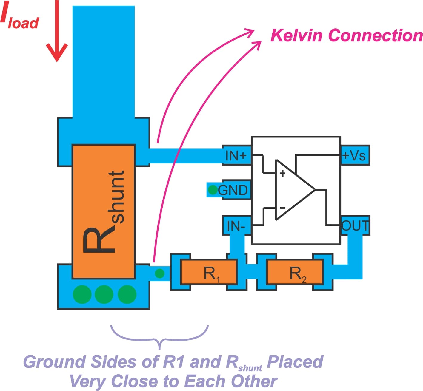
Figure 9.
Note that Kelvin connection is used for sensing the voltage across the shunt resistor. Also, note that the ground sides of R1 and Rshunt are placed very close to each other. Keep in mind that there are several different pad layouts for Kelvin connection. You might need to consult the resistor manufacturer or do some experiments to decide the appropriate layout for your design.
You can find an example layout for an op-amp in the X2SON package in “How to lay out a PCB for high-performance, low-side current-sensing designs” from TI.
To see a complete list of my articles, please visit this page.
Related Content