 Facebook
 Google
 GitHub
 Linkedin
Minterm vs Maxterm Solution
So far we have been finding Sum-Of-Product (SOP) solutions to logic reduction problems. For each of these SOP solutions, there is also a Product-Of-Sums solution (POS), which could be more useful, depending on the application.
Before working a Product-Of-Sums solution, we need to introduce some new terminology. The procedure below for mapping product terms is not new to this chapter.
We just want to establish a formal procedure for minterms for comparison to the new procedure for maxterms.
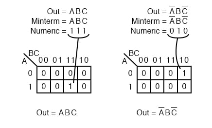
Minterm
A minterm is a Boolean expression resulting in 1 for the output of a single cell, and 0s for all other cells in a Karnaugh map, or truth table. If a minterm has a single 1 and the remaining cells as 0s, it would appear to cover a minimum area of 1s.
The illustration above left shows the minterm ABC, a single product term, as a single 1 in a map that is otherwise 0s. We have not shown the 0s in our Karnaugh maps up to this point, as it is customary to omit them unless specifically needed. Another minterm A’BC’ is shown above right.
The point to review is that the address of the cell corresponds directly to the minterm being mapped. That is, the cell 111 corresponds to the minterm ABC above left.
Above right we see that the minterm A’BC’ corresponds directly to the cell 010. A Boolean expression or map may have multiple minterms.
Referring to the above figure, Let’s summarize the procedure for placing a minterm in a K-map:
- Identify the minterm (product term) term to be mapped.
- Write the corresponding binary numeric value.
- Use binary value as an address to place a 1 in the K-map
- Repeat steps for other minterms (P-terms within a Sum-Of-Products).
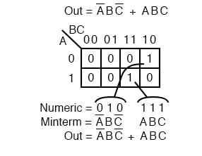
A Boolean expression will more often than not consist of multiple minterms corresponding to multiple cells in a Karnaugh map as shown above. The multiple minterms in this map are the individual minterms which we examined in the previous figure above.
The point we review for reference is that the 1s come out of the K-map as a binary cell address which converts directly to one or more product terms.
By directly we mean that a 0 corresponds to a complemented variable, and a 1 corresponds to a true variable. Example: 010 converts directly to A’BC’.
There was no reduction in this example. Though, we do have a Sum-Of-Products result from the minterms.
Referring to the above figure, Let’s summarize the procedure for writing the Sum-Of-Products reduced Boolean equation from a K-map:
- Form largest groups of 1s possible covering all minterms. Groups must be a power of 2.
- Write binary numeric value for groups.
- Convert binary value to a product term.
- Repeat steps for other groups. Each group yields a p-terms within a Sum-Of-Products.
Nothing new so far, a formal procedure has been written down for dealing with minterms. This serves as a pattern for dealing with maxterms.
Next we attack the Boolean function which is 0 for a single cell and 1s for all others.
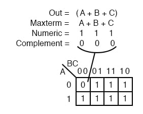
Maxterm
A maxterm is a Boolean expression resulting in a 0 for the output of a single cell expression, and 1s for all other cells in the Karnaugh map, or truth table. The illustration above left shows the maxterm (A+B+C), a single sum term, as a single 0 in a map that is otherwise 1s.
If a maxterm has a single 0 and the remaining cells as 1s, it would appear to cover a maximum area of 1s.
There are some differences now that we are dealing with something new, maxterms. The maxterm is a 0, not a 1 in the Karnaugh map. A maxterm is a sum term, (A+B+C) in our example, not a product term. It also looks strange that (A+B+C) is mapped into the cell 000.
For the equation Out=(A+B+C)=0, all three variables (A, B, C) must individually be equal to 0. Only (0+0+0)=0 will equal 0. Thus we place our sole 0 for minterm (A+B+C) in cell A,B,C=000 in the K-map, where the inputs are all 0 .
This is the only case which will give us a 0 for our maxterm. All other cells contain 1s because any input values other than ((0,0,0) for (A+B+C) yields 1s upon evaluation.
Referring to the above figure, the procedure for placing a maxterm in the K-map is:
- Identify the Sum term to be mapped.
- Write corresponding binary numeric value.
- Form the complement
- Use the complement as an address to place a 0 in the K-map
- Repeat for other maxterms (Sum terms within Product-of-Sums expression).
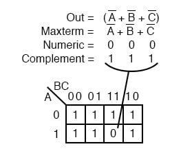
Another maxterm A’+B’+C’ is shown above. Numeric 000 corresponds to A’+B’+C’. The complement is 111. Place a 0 for maxterm (A’+B’+C’) in this cell (1,1,1) of the K-map as shown above.
Why should (A’+B’+C’) cause a 0 to be in cell 111? When A’+B’+C’ is (1’+1’+1’), all 1s in, which is (0+0+0) after taking complements, we have the only condition that will give us a 0. All the 1s are complemented to all 0s, which is 0 when ORed.
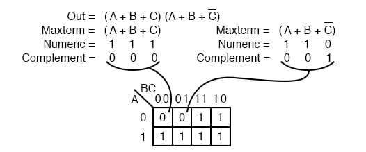
A Boolean Product-Of-Sums expression or map may have multiple maxterms as shown above. Maxterm (A+B+C) yields numeric 111 which complements to 000, placing a 0 in cell (0,0,0). Maxterm (A+B+C’) yields numeric 110 which complements to 001, placing a 0 in cell (0,0,1).
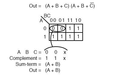
Now that we have the k-map setup, what we are really interested in is showing how to write a Product-Of-Sums reduction. Form the 0s into groups. That would be a group of two below. Write the binary value corresponding to the sum-term which is (0,0,X).
Both A and B are 0 for the group. But, C is both 0 and 1 so we write an X as a place holder for C. Form the complement (1,1,X). Write the Sum-term (A+B) discarding the C and the X which held its’ place.
In general, expect to have more sum-terms multiplied together in the Product-Of-Sums result. Though, we have a simple example here.
Let’s summarize the procedure for writing the Product-Of-Sums Boolean reduction for a K-map:
- Form largest groups of 0s possible, covering all maxterms. Groups must be a power of 2.
- Write binary numeric value for group.
- Complement binary numeric value for group.
- Convert complement value to a sum-term.
- Repeat steps for other groups. Each group yields a sum-term within a Product-Of-Sums result.
Examples
Example:
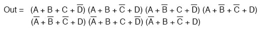
Simplify the Product-Of-Sums Boolean expression below, providing a result in POS form.

Solution:
Transfer the seven maxterms to the map below as 0s. Be sure to complement the input variables in finding the proper cell location.
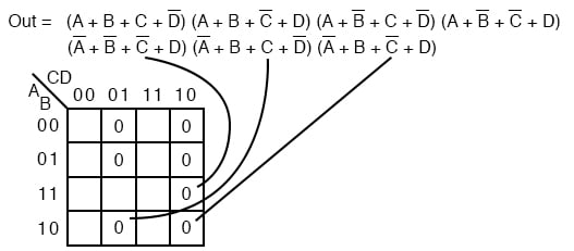
We map the 0s as they appear left to right top to bottom on the map above. We locate the last three maxterms with leader lines..
Once the cells are in place above, form groups of cells as shown below. Larger groups will give a sum-term with fewer inputs. Fewer groups will yield fewer sum-terms in the result.
We have three groups, so we expect to have three sum-terms in our POS result above. The group of 4-cells yields a 2-variable sum-term. The two groups of 2-cells give us two 3-variable sum-terms.
Details are shown for how we arrived at the Sum-terms above. For a group, write the binary group input address, then complement it, converting that to the Boolean sum-term. The final result is product of the three sums.
Example:
Simplify the Product-Of-Sums Boolean expression below, providing a result in SOP form.
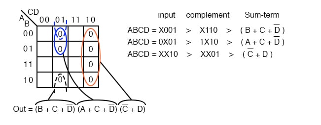
Solution: This looks like a repeat of the last problem. It is except that we ask for a Sum-Of-Products Solution instead of the Product-Of-Sums which we just finished. Map the maxterm 0s from the Product-Of-Sums given as in the previous problem, below left.
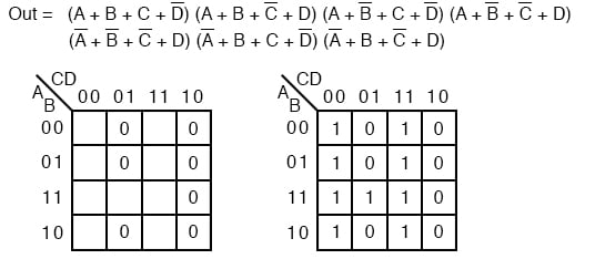
Then fill in the implied 1s in the remaining cells of the map above right.
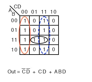
Form groups of 1s to cover all 1s. Then write the Sum-Of-Products simplified result as in the previous section of this chapter. This is identical to a previous problem.
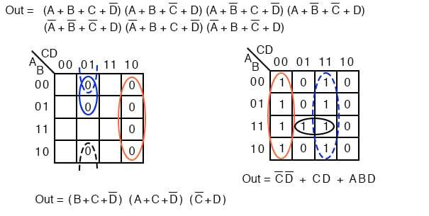
Above we show both the Product-Of-Sums solution, from the previous example, and the Sum-Of-Products solution from the current problem for comparison.
Which is the simpler solution? The POS uses 3-OR gates and 1-AND gate, while the SOP uses 3-AND gates and 1-OR gate. Both use four gates each.
Taking a closer look, we count the number of gate inputs. The POS uses 8-inputs; the SOP uses 7-inputs. By the definition of minimal cost solution, the SOP solution is simpler.
This is an example of a technically correct answer that is of little use in the real world.
The better solution depends on complexity and the logic family being used. The SOP solution is usually better if using the TTL logic family, as NAND gates are the basic building block, which works well with SOP implementations.
On the other hand, A POS solution would be acceptable when using the CMOS logic family since all sizes of NOR gates are available.
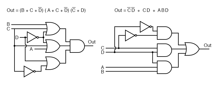
The gate diagrams for both cases are shown above, Product-Of-Sums left, and Sum-Of-Products right.
Below, we take a closer look at the Sum-Of-Products version of our example logic, which is repeated at left.
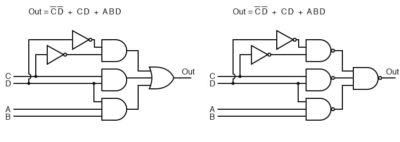
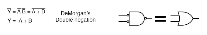
Above all AND gates at left have been replaced by NAND gates at right.. The OR gate at the output is replaced by a NAND gate. To prove that AND-OR logic is equivalent to NAND-NAND logic, move the inverter invert bubbles at the output of the 3-NAND gates to the input of the final NAND as shown in going from above right to below left.
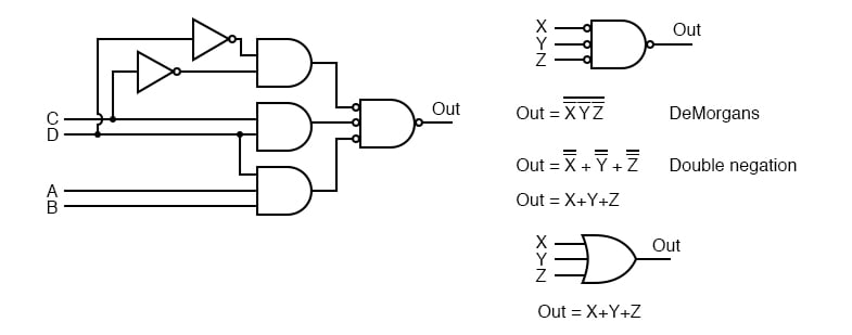
Above right we see that the output NAND gate with inverted inputs is logically equivalent to an OR gate by DeMorgan’s theorem and double negation.
This information is useful in building digital logic in a laboratory setting where TTL logic family NAND gates are more readily available in a wide variety of configurations than other types.
The Procedure for constructing NAND-NAND logic, in place of AND-OR logic is as follows:
- Produce a reduced Sum-Of-Products logic design.
- When drawing the wiring diagram of the SOP, replace all gates (both AND and OR) with NAND gates.
- Unused inputs should be tied to logic High.
- In case of troubleshooting, internal nodes at the first level of NAND gate outputs do NOT match AND-OR diagram logic levels, but are inverted. Use the NAND-NAND logic diagram. Inputs and final output are identical, though.
- Label any multiple packages U1, U2,.. etc.
- Use data sheet to assign pin numbers to inputs and outputs of all gates.
Example:
Let us revisit a previous problem involving an SOP minimization. Produce a Product-Of-Sums solution. Compare the POS solution to the previous SOP.
Solution:
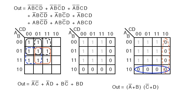
Above left we have the original problem starting with a 9-minterm Boolean unsimplified expression. Reviewing, we formed four groups of 4-cells to yield a 4-product-term SOP result, lower left.
In the middle figure, above, we fill in the empty spaces with the implied 0s. The 0s form two groups of 4-cells. The solid blue group is (A’+B), the dashed red group is (C’+D). This yields two sum-terms in the Product-Of-Sums result, above right Out = (A’+B)(C’+D)
Comparing the previous SOP simplification, left, to the POS simplification, right, shows that the POS is the least cost solution. The SOP uses 5-gates total, the POS uses only 3-gates.
This POS solution even looks attractive when using TTL logic due to simplicity of the result. We can find AND gates and an OR gate with 2-inputs.
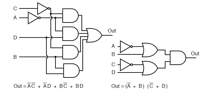
The SOP and POS gate diagrams are shown above for our comparison problem.
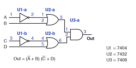
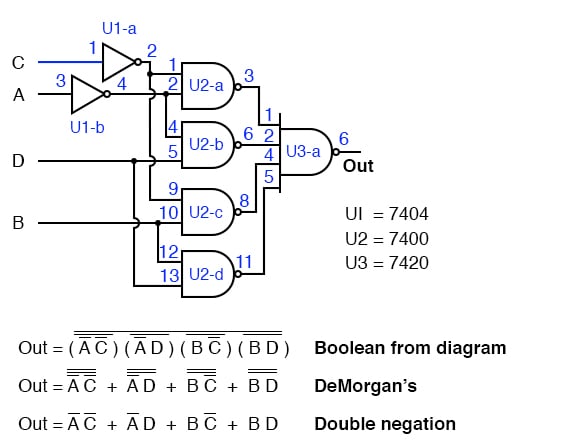
Given the pin-outs for the TTL logic family integrated circuit gates below, label the maxterm diagram above right with Circuit designators (U1-a, U1-b, U2-a, etc), and pin numbers.
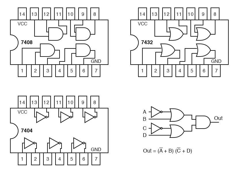
Each integrated circuit package that we use will receive a circuit designator: U1, U2, U3. To distinguish between the individual gates within the package, they are identified as a, b, c, d, etc.
The 7404 hex-inverter package is U1. The individual inverters in it are are U1-a, U1-b, U1-c, etc. U2 is assigned to the 7432 quad OR gate. U3 is assigned to the 7408 quad AND gate.
With reference to the pin numbers on the package diagram above, we assign pin numbers to all gate inputs and outputs on the schematic diagram below.
We can now build this circuit in a laboratory setting. Or, we could design a printed circuit board for it. A printed circuit board contains copper foil “wiring” backed by a non conductive substrate of phenolic, or epoxy-fiberglass.
Printed circuit boards are used to mass produce electronic circuits. Ground the inputs of unused gates.
Label the previous POS solution diagram above left (third figure back) with Circuit designators and pin numbers. This will be similar to what we just did.
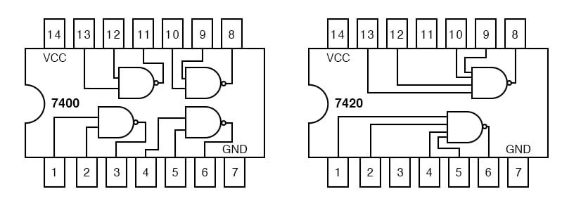
We can find 2-input AND gates, 7408 in the previous example. However, we have trouble finding a 4-input OR gate in our TTL catalog.
The only kind of gate with 4-inputs is the 7420 NAND gate shown above right.
We can make the 4-input NAND gate into a 4-input OR gate by inverting the inputs to the NAND gate as shown below. So we will use the 7420 4-input NAND gate as an OR gate by inverting the inputs.
We will not use discrete inverters to invert the inputs to the 7420 4-input NAND gate, but will drive it with 2-input NAND gates in place of the AND gates called for in the SOP, minterm, solution.
The inversion at the output of the 2-input NAND gates supply the inversion for the 4-input OR gate.
The result is shown above. It is the only practical way to actually build it with TTL gates by using NAND-NAND logic replacing AND-OR logic.
RELATED WORKSHEETS:


if you still do a wrong k-map, lets troubleshoot your maths
https://www.youtube.com/watch?v=5_dxk2FqEnY&t