Facebook
 Google
 GitHub
 Linkedin
How to Demodulate Digital Phase Modulation
In the previous two pages we discussed systems for performing demodulation of AM and FM signals that carry analog data, such as (non-digitized) audio. Now we are ready to look at how to recover original information that has been encoded via the third general type of modulation, namely, phase modulation.
However, analog phase modulation is not common, whereas digital phase modulation is very common. Thus, it makes more sense to explore PM demodulation in the context of digital RF communication. We’ll explore this topic using binary phase shift keying (BPSK); however, it’s good to be aware that quadrature phase shift keying (QPSK) is more relevant to modern wireless systems.
As the name implies, binary phase shift keying represents digital data by assigning one phase to binary 0 and a different phase to binary 1. The two phases are separated by 180° to optimize demodulation accuracy—more separation between the two phase values makes it easier to decode the symbols.
Multiply and Integrate—and Synchronize
A BPSK demodulator consists primarily of two functional blocks: a multiplier and an integrator. These two components will produce a signal that corresponds to the original binary data. However, synchronization circuitry is also needed, because the receiver must be able to identify the boundary between bit periods. This is an important difference between analog demodulation and digital demodulation, so let’s take a closer look.
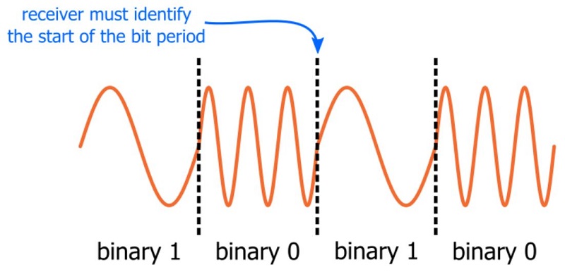
This diagram shows a frequency-shift-keying signal, but the same concept applies to digital phase modulation and digital amplitude modulation.
In analog demodulation, the signal doesn’t really have a beginning or an end. Imagine an FM transmitter that is broadcasting an audio signal, i.e., a signal that continuously varies according to the music. Now imagine an FM receiver that is initially turned off. The user can power up the receiver at any moment in time, and the demodulation circuitry will begin extracting the audio signal from the modulated carrier. The extracted signal can be amplified and sent to a speaker, and the music will sound normal. The receiver has no idea if the audio signal represents the beginning or end of a song, or if the demodulation circuitry starts functioning at the beginning of a measure, or right on the beat, or in between two beats. It doesn’t matter; each instantaneous voltage value corresponds to one exact moment in the audio signal, and the sound is re-created when all of these instantaneous values occur in succession.
With digital modulation, the situation is completely different. We’re not dealing with instantaneous amplitudes but rather a sequence of amplitudes that represents one discrete piece of information, namely, a number (one or zero). Each sequence of amplitudes—called a symbol, with a duration equal to one bit period—must be distinguished from the preceding and following sequences: If the broadcaster (from the above example) were using digital modulation and the receiver powered up and started demodulating at a random point in time, what would happen? Well, if the receiver happened to start demodulating in the middle of a symbol, it would be trying to interpret half of one symbol and half of the following symbol. This would, of course, lead to errors; a logic-one symbol followed by a logic-zero symbol would have an equal chance of being interpreted as a one or a zero.
Clearly, then, synchronization must be a priority in any digital RF system. One straightforward approach to synchronization is to precede each packet with a predefined “training sequence” consisting of alternating zero symbols and one symbols (as in the above diagram). The receiver can use these one-zero-one-zero transitions to identify the temporal boundary between symbols, and then the rest of the symbols in the packet can be interpreted properly simply by applying the system’s predefined symbol duration.
The Effect of Multiplication
As mentioned above, a fundamental step in PSK demodulation is multiplication. More specifically, we multiply an incoming BPSK signal by a reference signal with frequency equal to the carrier frequency. What does this accomplish? Let’s look at the math; first, the product identify for two sine functions:
$$\sin(x)*\sin(y)=\frac{1}{2}(\cos(x-y)-\cos(x+y))$$
If we turn these generic sine functions into signals with a frequency and phase, we have the following:
$$\sin(\omega_C+\theta_1)*\sin(\omega_C+\theta_2)=\frac{1}{2}[\cos(\omega_C+\theta_1-(\omega_C+\theta_2))-\cos(\omega_C+\theta_1+\omega_C+\theta_2)]$$
Simplifying, we have:
$$\sin(\omega_C+\theta_1)*\sin(\omega_C+\theta_2)=\frac{1}{2}[\cos(\theta_1-\theta_2)-\cos(2\omega_C+(\theta_1+\theta_2))]$$
So when we multiply two sinusoids of equal frequency but different phase, the result is a sinusoid of double the frequency plus an offset that depends on the difference between the two phases. The offset is the key: If the phase of the received signal is equal to the phase of the reference signal, we have cos(0°), which equals 1. If the phase of the received signal is 180° different from the phase of the reference signal, we have cos(180°), which is –1. Thus, the output of the multiplier will have a positive DC offset for one of the binary values and a negative DC offset for the other binary value. This offset can be used to interpret each symbol as a zero or a one.
Simulation Confirmation
The following BPSK modulation-and-demodulation circuit shows you how you can create a BPSK signal in LTspice:
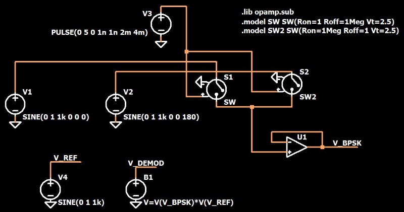
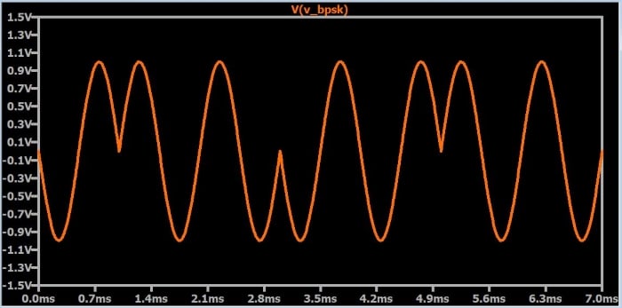
Two sine sources (one with phase = 0° and one with phase = 180°) are connected to two voltage-controlled switches. Both switches have the same square-wave control signal, and the on and off resistances are configured such that one is open while the other is closed. The “output” terminals of the two switches are tied together, and the op-amp buffers the resulting signal, which looks like this:
Next, we have a reference sinusoid (V4) with frequency equal to the frequency of the BPSK waveform, and then we use an arbitrary behavioral voltage source to multiply the BPSK signal by the reference signal. Here is the result:
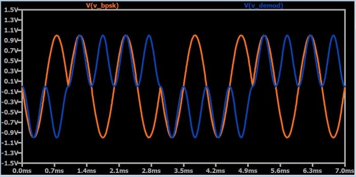
As you can see, the demodulated signal is double the frequency of the received signal, and it has a positive or negative DC offset according to the phase of each symbol. If we then integrate this signal with respect to each bit period, we will have a digital signal that corresponds to the original data.
Coherent Detection
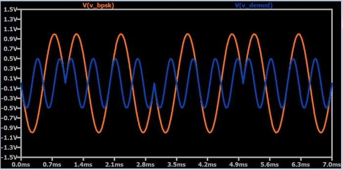
In this example, the phase of the receiver’s reference signal is synchronized with the phase of the incoming modulated signal. This is easily accomplished in a simulation; it’s significantly more difficult in real life. Furthermore, as discussed in this page under “Differential Encoding,” ordinary phase shift keying cannot be used in systems that are subject to unpredictable phase differences between transmitter and receiver. For example, if the receiver’s reference signal is 90° out of phase with the transmitter’s carrier, the phase difference between the reference and the BPSK signal will always be 90°, and cos(90°) is 0. Thus, the DC offset is lost, and the system is completely nonfunctional.
This can be confirmed by changing the phase of the V4 source to 90°; here is the result:
Summary
- Digital demodulation requires bit-period synchronization; the receiver must be able to identify the boundaries between adjacent symbols.
- Binary-phase-shift-keying signals can be demodulated via multiplication followed by integration. The reference signal used in the multiplication step has the same frequency as the transmitter’s carrier.
- Ordinary phase-shift-keying is reliable only when the phase of the receiver’s reference signal can maintain synchronization with the phase of the transmitter’s carrier.