Facebook
 Google
 GitHub
 Linkedin
Decision Feedback Equalization: the Technique Driving DDR5’s Blazing-Fast Transfer Rates
As an EE, you might wonder how DDR5 can support blazing-fast transfer rates. One factor is an equalization technique called decision feedback equalization (DFE).
As the number of cores in a modern processor increases, higher memory bandwidth is required to unleash the computational power of the CPU. Boosting memory bandwidth is the primary driver for developing DDR5, the fifth generation of DDR technology.
The previous generational updates of DDR improved data transfer rate as well; however, they were driven by the need to reduce memory power consumption in mobile and data center applications. The figure below gives some basic parameters of different DDR generations.

Generational differences in DRAM specifications. Image used courtesy of SK hynix
Compared to DDR4, DDR5 will double the data transfer rate while supporting a larger memory density. DDR5 is expected to be the next mainstream computer memory standard. According to Omdia, an independent analyst and consultancy firm, DDR5 will possess 10% of the global DRAM market share in 2022. This will increase to 43% in 2024.
SK hynix Launches the First DDR5 DRAM
SK hynix has recently launched its DDR5 DRAM specifically designed for big data, artificial intelligence, and machine learning applications. With a transfer rate of 4,800 ~ 5,600 megabit-per-second (Mbps), the new product can improve the transfer rate by a factor of 1.8 compared to a DDR4-based solution.

SK hynix's new DDR5 DRAM module. Image used courtesy of SK hynix
Running from 1.1 V, the new memory cuts down power consumption by 20% compared to a DDR4 product that is operated with a 1.2 V supply. The company claims that the new memory improves the reliability of applications by 20 times through error-correcting code (ECC) that is implemented inside the memory chip.
As an EE, you might wonder how DDR5 can support these blazing-fast transfer rates. There are several different techniques that are used to enable these transfer rates. One of the key techniques is an equalization technique called decision feedback equalization that is briefly discussed in the rest of this article.
Equalization Can Cancel Channel Non-Ideal Response
A typical controller-memory interface is shown below.

The interface of a typical memory controller. Image used courtesy of Jose E. Schutt-Aine
Copper resistance and dielectric loss attenuate the signal as it travels over the PCB trace. The loss is frequency-dependent and has an overall low-pass filtering effect. The black curve in the figure below shows the frequency response of an example PCB trace.

Graph depicting channel equalization. Image used courtesy of Jose E. Schutt-Aine
Channel response variation with frequency distorts the signal and leads to intermodulation distortion (ISI). The end result is a data-dependent timing jitter on the signal transition edges that leads to a closed eye diagram.

Intermodulation distortion can lead to bad eye diagrams, high jitter, and high bit-error rates. Image used courtesy of Teledyne LeCroy
To mitigate this effect, we can apply a compensating filter that cancels the channel frequency response variation and leads to an overall flat response (“equalized response” in the frequency response figure). Note that equalization is a general technique and there are standalone redriver chips based on this technique that can be used when dealing with long PCB traces.
Equalization in the DDR Ecosystem
High-speed DDR systems rely on different equalization techniques to improve signal integrity at high data rates. Decision feedback equalization (DFE) is one of the key equalization techniques that enables DDR5 to support higher IO speeds.
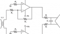
In DDR4, DFE is utilized to address signal integrity issues of the data channel (DQ bus) only. However, with DDR5, even the lower-speed command address (CA) bus requires DFE to ensure reliable signal reception. Equalization circuitry might be implemented in the DRAM and/or in the memory controller. The figure below shows an analog implementation of a two-tap DFE.

Diagram of a two-tap DFE architecture. Image used courtesy of Behzad Razavi
In this example, the received signal is delayed by the two flip-flops. The output of the delay line is weighted by h1 and h2 and fed back to the input. The coefficients are chosen based on the channel response. For example, we can monitor the eye diagram at the summer output and choose the coefficients to maximize the eye diagram height.
For an intuitive explanation of the DFE operation, you can refer to “The Decision-Feedback Equalizer” by Behzad Razavi.
DFE Limitations
Although DFE is a neat solution to achieve high data rates, it has its own disadvantages. DFE adds extra delay to the signal path and consequently, increases memory access time. Besides, DFE can cancel only a portion of the ISI distortion (it can only compensate for post cursor ISI).
To have a more effective solution, DFE should be combined with other equalization techniques such as FFE (feed‐forward equalization). Furthermore, noise and crosstalk components that appear at the flip-flop inputs can lead to false decisions at the flip-flop outputs and lead to erroneous operation of the circuit.
Related Content