Facebook
 Google
 GitHub
 Linkedin
How CMOS Image Sensors Are Making Strides in Pixel Count and Size
Companies like Sony and OmniVision continue to develop advanced CMOS image sensors, while the Emmys pay respect to Kodak as one of the forerunners in digital imaging.
For many years, charge-coupled devices (CCD) were the dominant technology used in digital imaging, possessing superior figures of merit in sensitivity, speed, and reliability. However, as fabrication processes have improved, CMOS-based technologies have overtaken CCD. Noticing this trend, Sony in 2015 began the process of discontinuing CCD development over the next ten years.
CMOS image sensors have come a long way since Kodak's early days of intra-pixel charge transfer CMOS image sensors, which were awarded a Technology and Engineering Emmy this week.

Decades of breakthrough technologies by Kodak paved the way for current CMOS-based image sensors. Image used courtesy of YMCinema
As a testament to the accelerating innovations in this field, Sony and OmniVision have both recently released new CMOS image sensors focused on different markets: industrial imaging and medical imaging, respectively.

Diagram of a CMOS-based image sensor made up of a photosensitive chip, wire-bonded to an IC package. Image used courtesy of Lucid Vision Labs
Sizing up these new devices can offer a window into the direction of digital imaging and the subsequent impact on engineers working with CMOS image sensors.
Sony’s High-resolution Image Sensor for Industrial Imaging
This week, Sony announced a large-format CMOS image sensor, the IMX661, claimed to feature the "industry’s highest effective pixel count" at 127.68 megapixels. What exactly does this figure mean for engineers working in industrial imaging?
Expanding Die Size Without Compromising Resolution
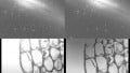
There is an inverse relationship between pixel size sensitivity (the individual active elements of the sensor) and resolution—relative to die size. The result is called image format.

The new Sony 127.68 megapixel image sensor IMX661, which is said to offer increased sensor resolution at 3.5 μm pixel size. Image used courtesy of Sony
The popular standard in optic mounting is called a C-mount, utilizing a 1.1-inch format sensor, which does not appear to fit the 3.6-type package of the IMX661. Sony appears to be marketing its newest device as an alternative to the C-mount-style optics but at a significantly higher image resolution.
The Value of Global Shutter
The IMX661 sensor is designed to offer a global shutter with Sony’s proprietary technology “Pregius." In contrast to rolling shutter, global shutter allows sensors to capture undistorted images of high-speed objects.

Global shutter is a feature that combats image distortion in objects that are moving relative to the pixel column. Image used courtesy of Lucid Vision Labs
While the readout into the processing unit is still sequential, the photosensitive elements are exposed uniformly in a global shutter, ensuring that a scene is sampled as a single frame in time.
Refining ADC Conversion Resolution
Reviewing the key technical specifications for the IMX661 reveals industry-standard voltages (3V3A,1V2D, and 1V8 for the interface) as well as the capability for various frame rates by selecting a 10-bit to 14-bit ADC resolution.
The ability to refine the ADC conversion resolution offers a significant amount of design variability for applications in fixed cameras vs. mobile cameras, such as those in vehicles.
OmniVision's Medical-grade Sensors Reduce Invasive Diagnostics
While Sony is thinking big with its optics, OmniVision is shrinking its family of medical-grade sensors while upholding high standards for optical format, resolution, and power demand.
Record-breaking Sensor Size
In a press release for the company's newest CMOS image sensor, the OHOTA10, OmniVision claims that it has broken its own Guinness world record for size with the "world's smallest commercial image sensor." The new OHOTA10 reduces the size of the previous-generation OV6948 from 575 μm2 to 550 μm2.

The OHOTA10 offers an iterative reduction in size over the OV6948, but with double the resolution. Image used courtesy of OmniVision
Built for Minimally-invasive Probes
OmniVision envisions this new optic package opening doors for designers to create smaller minimally-invasive probes for diagnostic applications.
“These state-of-the-art CIS [CMOS image sensors] technologies are meeting today’s key endoscopy requirements to support doctors in their diagnostic processes or surgical procedures with higher image quality and better contrast while increasing patient comfort," says Chenmeijing Liang, technology and market analyst of imaging at Yole Développement.

OmniVision says the new image sensor increases image quality while reducing power consumption in endoscopes and catheters. Image used courtesy of OmniVision
"They also allow less invasive imaging techniques for neurologic, ENT or pediatric applications without altering image resolution."
Upping Resolution, Cutting Power Consumption
Additionally, a pixel size reduction of 42% allows for a two-times increase in the optical resolution despite the reduction in package size.
However, for engineers designing these systems, the exciting improvements include a 20% improvement in power consumption (25 mW to 20 mW) as well as an optical format reduction from 1/36” to 1/31”, which facilitates the smaller package size.
The March of Progress for CMOS Optics
As evidenced in these announcements, CMOS-based technologies offer superior noise immunity and dynamic ranges because they integrate amplifiers and convert analog-to-digital signals at the pixel column.
It took decades for CMOS-based image sensors to overtake CCD as the principal optical sensor. However, with improved processes for the fabrication of optical wafers and reduced pixel sizes, CMOS has come out on top.
Designing digital imaging systems in both industrial and medical fields present unique challenges for designers. Do you have experience working with such technologies? Share your thoughts in the comments below.