Facebook
 Google
 GitHub
 Linkedin
Two for One: A Buck Regulator and an LDO in a Single Package from Analog Devices
Called a Micro PMU, this IC from Analog Devices offers a 3A buck regulator and a 3A ultralow-noise LDO in a single package.
Called a Micro PMU, this IC from Analog Devices offers a 3A buck regulator and a 3A ultralow-noise LDO in a single package.
Analog Devices recently announced their new ADP5003 low-noise DC power supply system. They describe it as a micro PMU (power management unit) given that it combines a buck regulator (i.e., a step-down regulator) along with an ultralow-noise LDO (low dropout) regulator.
This IC offers a host of features and, consequently, implementation is somewhat complicated. Also, it is not exactly a low-pin-count device. It comes in a 32-pin, 5 × 5 mm LFCSP (leadframe chip scale package). This means that, in order to take advantage of what this PMU offers, you'll have to put some thought—perhaps considerable thought—into exactly how you want to configure this IC for your design.
_block-diagram.jpg)
Figure 1. The ADP5003 is a 32-pin device that includes both a buck regulator and an LDO. Taken from the datasheet (PDF).
_IC-pinout.jpg)
Figure 2. The ADP5003 is available only in a 32-pin 5 × 5 mm LFCSP (leadframe chip scale package). Diagram taken from the datasheet (PDF).
Two Options for Controlling the Two Voltage Regulators
There are two modes of operation when it comes to controlling the two regulators: one scheme is called Independent Mode while the other is referred to as Adaptive Mode.
Independent Mode
As the name implies, this mode of operation allows both the LDO and the buck regulator to function as two standalone devices to generate two voltage rails from a single voltage supply. This simply means that each voltage regulator has separate pins for input voltage, output voltage, and voltage-setting resistors. Note that the input voltage range is not the same for each of these two regulators: the LDO's input voltage range is 0.65 to 5 V, and the input voltage range of the buck regulator is 4.2 to 15 V. Additionally, and perhaps not surprisingly, the output-voltage ranges are different as well:
- LDO VOUT: 0.6 to 3.3 V
- Buck regulator VOUT: 0.6 to 5.0 V
The two figures below depict how each regulator is configured in independent mode.
_indepedent_mode_Buck.jpg)
Figure 3. Buck regulator configuration in independent mode, from the datasheet (PDF).
_indepedent_mode_LDO.jpg)
Figure 4. LDO configuration in independent mode, from the datasheet (PDF).
Adaptive Mode
When configured for adaptive mode (see figure below), the buck regulator’s output feeds the input of the LDO, and the buck regulator’s output voltage is controlled such that it provides the optimal amount of LDO headroom, which results in better LDO efficiencies. This adaptive mode also optimizes the LDO headroom voltage when the POL (point of load) remote sense feedback option is used. As a reminder, POL remote sensing is utilized to compensate for the PCB's trace impedance when delivering high output currents.
_adaptive_mode.jpg)
Figure 5. A figure from the datasheet showing the ADP5003 configured for adaptive mode.
When the ADP5003 is configured for adaptive mode, the headroom profile used by the adaptive headroom control optimizes the efficiency of the overall system and results in consistent PSRR (power supply rejection ratio) despite varying load conditions (see the figure below).
_adaptive_mode_PSRR.jpg)
Figure 6. In adaptive mode, the ADP5003 attempts to deliver a consistent PSRR across the load range. From the datasheet.
IC Protections
The ADP5003 comes with the common protection features that we’re used to seeing on voltage regulator ICs:
- current-limit protection
- short-circuit protection
- UVLO (under voltage lockout)
- TSD (thermal shutdown)
Regarding the TSD: It's a bit unclear why the TSD limit is set to 155°C (TJ) when the absolute operating junction temperature range (TJ) is -40°C to 125°C and is accompanied by the warning, "Stresses at or above those listed under Absolute Maximum Ratings may cause permanent damage to the product." See the figures below.
_abs_temp_range.jpg)
Figure 7. The upper end of the absolute maximum operating junction temperature range is 125°C. Table taken from the datasheet.
_TSD.jpg)
Figure 8. The datasheet indicates that the TSD (thermal shutdown) threshold is 155°C, which exceeds the absolute maximum operating junction temperature of 125°C
The way I read the specifications and the warning is as follows: The ADP5003 must exceed the absolute operating junction temperature (TJ) of 125°C—and risk causing permanent damage to itself—before the TSD (155°C) limit is reached. In other words, it seems that once the TSD limit is reached, the device itself has already been compromised and may be permanently damaged. Strange.
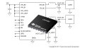
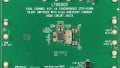
An Evaluation Board
Analog Devices has made an evaluation board available for demonstrating the features and functionalities of their new ADP5003 buck regulator plus LDO. So if you're interested in testing this new micro PMU, this eval board should prove useful.
_demo_board.jpg)
Figure 9. The evaluation board for the ADP5003. Image courtesy of the User Guide (PDF).
Have you had a chance to use the ADP5003 or its evaluation board? If so, leave a comment and tell us about your experiences.
Related Content