Facebook
 Google
 GitHub
 Linkedin
Improving ADC SFDR Using Dithering for Communication System Applications
Learn more about dithering, namely improving the spurious-free dynamic range (SFDR) of an analog-to-digital converter (ADC) that exhibits differential nonlinearity (DNL) errors.
In a previous article, we discussed how dithering can be used to improve the performance of an ideal quantizer by breaking up the statistical correlation between the quantization error and the input signal. By ideal, we mean that the ADC transfer function has uniform steps. Put differently, the ideal ADC has zero DNL error. This application of dithering is particularly important in radio receivers that need a high SFDR.
In this article, we’ll discuss another important application of dithering, namely improving the SFDR of a real-world A/D converter, like the AD6645, that exhibits DNL errors. This application of dithering is particularly important in today’s radio receivers that require a high SFDR.
ADC Static and Dynamic Linearity
Before jumping in, let's first have a quick review of the main limitations to increasing the ADC linearity. Although ADCs use different architectures and circuit implementations, they have two main nonlinearity sources: the sample and hold (S/H) circuit and the encoder portion of the ADC. Part of the S/H nonlinearity stems from the fact that it has a limited slew rate and might not be able to follow the input quickly enough when the input is a high-frequency signal with a large amplitude. The lack of S/Hs that exhibit adequate slew rate is a key reason why many ADCs fail to provide a high SFDR above several megahertz of signal bandwidth. This also explains why the nonlinearity of the S/H is frequency-dependent. The S/H plays a key role in determining the dynamic (or AC) linearity of the ADC.
The other nonlinearity source is the ADC encoder portion. For a given ADC phase, the encoder portion mostly deals with a DC signal because it is placed after the S/H. Therefore, the encoder nonlinearity contributes to the static (or DC) nonlinearity of the system. This component of nonlinearity doesn’t ideally change with frequency. Static nonlinearity is characterized by the DNL and INL (integral nonlinearity) errors in ADC’s transfer function. The term “static nonlinearity” might be a misnomer in the sense that this nonlinearity component doesn’t affect only DC signals, it also degrades linearity when dealing with AC signals.
Note Which Nonlinearity Type is the Dominant One!
Another important thing to keep in mind for this article is that, with many ADCs, the S/H is the dominant source of nonlinearity. In this case, the harmonic distortion performance degrades rapidly as the input approaches the Nyquist frequency. If the S/H is the limiting factor, there is nothing that can be done externally to significantly improve the ADC linearity. However, some ADCs are specifically designed with a wideband, highly linear front end. This makes the encoder portion the main source of nonlinearity. With such ADCs, we can use the dithering technique to improve the ADC SFDR. Before examining this application of dithering, let’s take a closer look at the nonlinearity error introduced by the ADC static transfer function.
Transfer Function Nonlinearity—a Deterministic Error
To better understand static nonlinearity, we’ll examine the nonlinearity error introduced by the transfer function shown in Figure 1 as an example.

Figure 1. Example transfer function introducing a nonlinearity error [click image to enlarge].
The red curve in the above figure shows a nonlinear 4-bit ADC, while the blue curve shows the ideal 4-bit response. If we use the above characteristic curves to digitize a 1.11 kHz sinusoid sampled at 4 MHz, we’ll obtain the following waveforms in Figure 2.
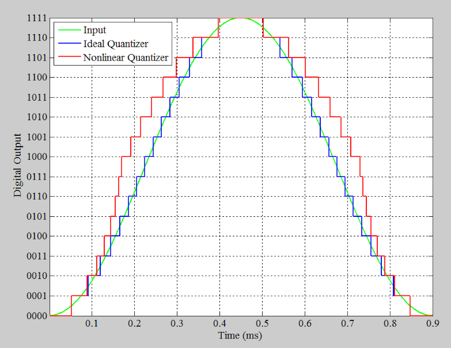
Figure 2. Waveforms of a digitized 1.11 kHz sinusoid sampled at 4 MHz [click image to enlarge].
In Figure 2, the green curve shows the input, while the blue and red curves are the outputs of the ideal and nonlinear transfer functions, respectively. By subtracting the blue curve from the red one, we can determine the nonlinearity error introduced by the non-ideal response. This is shown by the red curve in Figure 3.
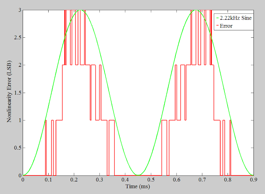
Figure 3. Plot showing the nonlinearity error introduced by the non-idea response [click image to enlarge].
The error introduced by the transfer function nonlinearity is a deterministic error. This means that, for a given input voltage, the error is always the same. For example, referring to Figure 1, we observe that an input of 6 LSBs (least significant bits) always leads to an output that is 3 LSBs higher than the ideal value. This deterministic behavior creates a correlation between the input and the error. If the input is at a particular frequency, we expect the error to have strong frequency components at some specific frequencies related to the input.
Figure 3 can help you better understand this situation. In this case, the error waveform is not exactly periodic; however, the overall shape of the error seems to repeat itself in a regular fashion. Namely, there are two repetitions in one period of the input signal. This suggests that the error has a strong component at the 2nd harmonic of the input. To better visualize this, the figure also plots a sine wave at 2.22 kHz (2nd harmonic). As you can see, the sine wave approximates the trend in the overall shape of the error waveform.
Taking the fast Fourier transform (FFT) of the nonlinear response output, we obtain the spectrum below in Figure 4, which shows only the DC to 50 kHz range.
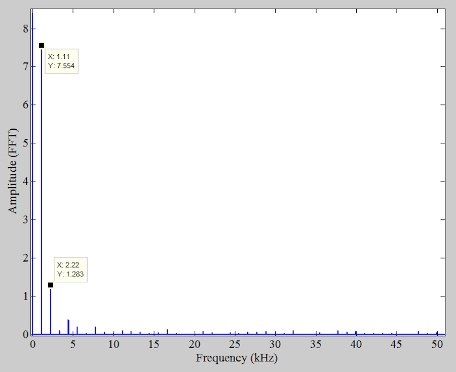
Figure 4. Plot showing the nonlinear response output from the DC to 50 kHz range [click image to enlarge].
The FFT result confirms that the 2nd harmonic is the dominant frequency component of the nonlinear response. It’s worthwhile to mention that the frequency of the dominant harmonic component depends on the INL shape of the ADC. With the nonlinearity shown in Figure 1, which is sometimes referred to as bow-shaped INL, the 2nd harmonic is the dominant one. With an S-shaped INL, the 3rd harmonic is the dominant frequency component of the error. For a discussion on the effect of INL shape on the frequency spectrum of a D/A converter (DAC or digital-to-analog converter), please refer to this article.
Breaking the Correlation Between ADC Error and Input
If we add a relatively large, random signal to the input so that the overall input of the ADC changes between different steps of the ADC transfer function in an unpredictable way, we can somewhat reduce the deterministic distortion. This concept is illustrated in Figure 5.
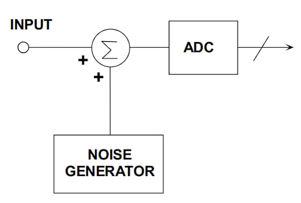
Figure 5. A basic diagram showing the ADC input changes during the ADC transfer function steps. Image used courtesy of Analog Devices
With the random signal (or the dither signal) added, a given input is not always translated to the same output level. Therefore, the error can change over time even if the input is constant. As an example, consider applying an input of 6 LSBs to the transfer function in Figure 1. Without dither, the error is always 3 LSBs. Now consider the dithered case. Assume that the dithered signal is occasionally equal to 2 LSBs. At 2 LSBs, the nonlinearity error becomes zero. Since the error changes between 0 and 3 LSBs, the error average is reduced compared to the undithered case. This simple example shows how dithering can eliminate the correlation between the input and the nonlinearity error and consequently reduce the deterministic distortion. Dithering achieves this by delocalizing or randomizing the DNL errors of the converter. By eliminating the error correlation with the input, harmonic components are spread into the noise floor, and the SFDR is improved.
Communications Systems Dithering Technique
The dithering technique is particularly helpful in communications systems. With many communications applications, the input can be a small signal well below the ADC full scale. This small signal exercises a relatively small number of the ADC codes. If these codes exhibit large DNL errors, the output will contain significant harmonic distortion.
Note that, with full-scale (or large) signals, the DNL error is inherently averaged to some extent. The reason is that a large signal exercises all codes of the ADC. As a result, an ADC that exhibits a full-scale SFDR of 88 dBFS might provide only 80 dBFS of SFDR when the signal amplitude is reduced to 20 dB below the full-scale value. In such cases, the dithering technique might help us maintain the SFDR performance of the ADC at low signal levels. It should be noted that since the input level is small, we can add the dither signal to the input without overdriving the ADC.
ADC Noise—Aren’t We Losing Information?
You might ask: aren’t we losing the information by adding a relatively large noise to the input signal? The answer is the information might seem to be lost in the time domain. However, a proper choice of the noise signal, along with signal processing techniques, allows us to reconstruct the original information. One solution is subtractive dithering. In this case, the basic diagram in Figure 5 is modified to the following one (Figure 6).
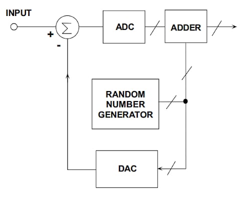
Figure 6. Subtractive dithering diagram. Image used courtesy of Analog Devices
In the subtractive method, the noise introduced to the input is added to the output with opposite polarity, zeroing out the net dithering noise at the system output. Another interesting technique, which is used in communications systems, is using a narrowband noise with frequency content outside of the bandwidth of the desired signal. A small bandwidth of a few hundred kHz is normally sufficient for the dither signal. Two possible locations for the out-of-band noise are near DC or slightly below the Nyquist frequency (fs/2, where fs is the sampling frequency). One of these two frequency zones is not used in most communications systems which can be used for dithering purposes. In this case, the dither can easily be filtered out at the output.
Playing With Our Hypothetical ADC
Let’s examine this technique using the transfer function in Figure 1. To do this, we apply a 1.11 kHz sinusoid with an amplitude of 2 LSBs and a DC value of 7.5 LSBs to this ADC. Such an input exercises the mid-range codes of the ADC. The output spectrum from slightly above 0 Hz to 30 kHz range is shown in Figure 7.

Figure 7. Another example plot of a 1.11 kHz sinusoid with a spectrum from slightly above 0 Hz to 30 kHz range [click image to enlarge].
With this particular input, there are several different harmonic components, but the dominant one is still the 2nd harmonic. Converting the values to decibels, we find the SFDR to be 17.47 dBc. To produce the dither signal, we can use Matlab “randn” function to produce a wideband Gaussian noise with 2 LSBs RMS (root-mean-square). Applying a bandpass filter with a passband of 100 kHz centered at 1.94 MHz, the wideband noise is converted into a narrowband dither slightly below fs/2. The spectrum of the dither signal is shown below in Figure 8.

Figure 8. An example spectrum of the dither signal [click image to enlarge].
Since the dither signal is the band-limited version of the original noise, we can use the following equation to determine the variance of the dither signal:
\[Variance \text{ } of \text{ } Dither = \frac{Filter \text{ }Bandwidth}{f_s/2} \times Noise \text{ } Variance\]
Plugging in the numbers, we obtain:
\[Variance \text{ } of \text{ } Dither = \frac{100 \text{ } kHz}{2 \text{ } MHz} \times 4 = 0.2\]
Taking the square root of this value, the RMS of the dither signal works out to 0.45 LSBs. The peak-to-peak value of the dither can be estimated as 6.6 x 0.45 = 2.97 LSBs (RMS Gaussian noise is converted to peak-to-peak by multiplying by 6.6). Note that the peak-to-peak value of the dither is small enough not to overdrive the ADC. With the dither applied, we obtain the following output spectrum (Figure 9).
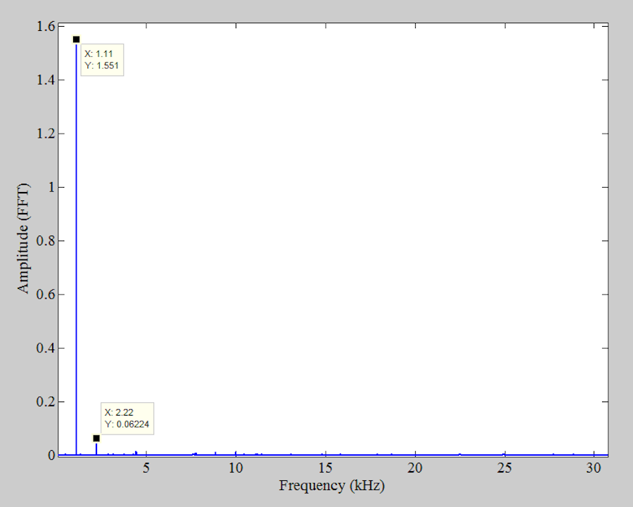
Figure 9. An output spectrum after applying RMS of the dither [click image to enlarge].
As can be seen, the harmonics are significantly suppressed. Converting the values to decibels, we obtain an SFDR of 27.9 dBc, which is an improvement of 10.43 dB compared to the undithered case. Dithering suppresses harmonic components by spreading the signal spurs into the noise floor.
Test Results of a Real-world ADC—the ADC3424
Figure 10 below shows the output spectrum of the ADC3424 for a 70 MHz input.
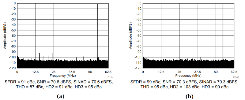
Figure 10. Output spectrums of the ADC3424 for a 70 MHz input. Image used courtesy of Texas Instruments
The ADC3424 provides the dither functionality as an internal feature. With the internal dither turned off, the SFDR is 91 dBc. However, with the internal dither activated, the spurs spread into the noise floor, and the SFDR increases to 99 dBc.
Dithering Technique Limitations
The proper level of dither that provides a significant improvement in ADC SFDR depends on the architecture and other properties of that specific ADC. The SFDR improvement also depends on the amplitude of the input signal as well as that of the dither. It should also be noted that beyond a certain level of noise, the SFDR might not improve significantly. As an example, consider the AD6645 from Analog Devices. This device uses a multistage architecture. With this type of ADC architecture, the DNL error has a repetitive pattern, and there are some spikes in the DNL plot as the input is swept over the ADC input range. Figure 11 below shows the DNL plot of the AD6645 over a small portion of its input range.
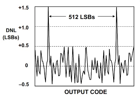
Figure 11. A DNL plot of the AD6645 over a small portion of its input range. Image used courtesy of Analog Devices
In the case of AD6645, the spikes occur every 512 LSBs. The experimentally found dither level suitable for this particular ADC is 1024 LSBs peak-to-peak or 155 LSBs RMS. Applying a larger dither doesn’t significantly improve the SFDR of the AD6645. For this ADC, the peak-to-peak value of the dither is equal to twice the code distance between two DNL spikes. However, we cannot conclude that this is a general rule for all multistage ADCs.
To learn more about the dithering technique, please refer to “Overcoming Converter Nonlinearities with Dither” from Analog Devices.
To see a complete list of my articles, please visit this page.
Related Content