Facebook
 Google
 GitHub
 Linkedin
Exploring Monolithic Thermocouple Signal Conditioning Using AD849x and LT1025
Learn about thermocouple signal conditioning and thermocouple nonlinearity through two different monolithic thermocouple amplifier solutions: the AD849x family and the LT1025.
The output of a thermocouple is a small voltage that typically changes by tens of microvolts per °C. This low-level signal requires significant amplification before it can be digitized by a typical ADC. Also, the thermocouple output should be compensated for the error from the non-zero cold junction temperature. In a previous article, we examined the discrete implementation of thermocouple signal conditioning circuits.
This article gives an overview of two different monolithic thermocouple solutions: the AD849x family and the LT1025. The next article in this series will continue this discussion and give an overview of the important features of the AD594/AD595 and the MAX6675.
Monolithic Thermocouple Amplifiers—AD849x Example
Diving in, let's take a look at a functional block diagram of the AD849x shown in Figure 1.
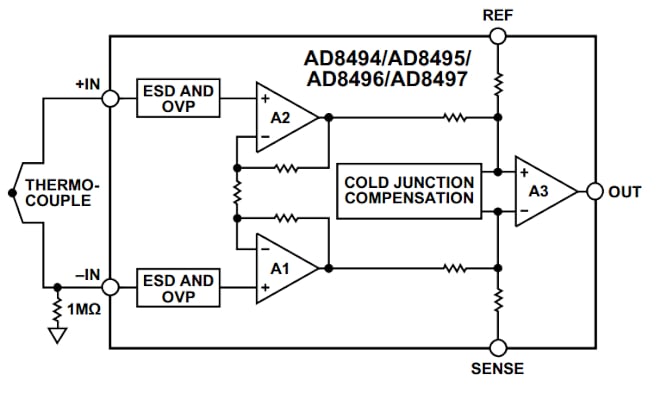
Figure 1. Block diagram of the AD849x. Image used courtesy of Analog Devices
This device includes a low offset, fixed-gain instrumentation amplifier and a built-in cold junction compensation (CJC) circuit. Each device in this family is factory-calibrated for J- or K-type thermocouples. The AD849x can directly convert the small output of the thermocouple to a high-level signal that changes by 5 mV/°C. The following equation can be used to find the hot junction temperature (TMJ) of the thermocouple:
\[T_{MJ}=\frac{V_{OUT}-V_{REF}}{5mV/°C}\]
Equation 1.
Where VREF is the voltage at the REF pin. For example, if the AD8494 produces an output of 250 mV and VREF = 0, the hot junction is at 50 °C.
Thermocouple Signal Conditioning: IC and Cold Junction at the Same Temperature
One general requirement that should be considered when working with monolithic thermocouple solutions is that these devices should be placed close to the cold junction of the thermocouple (Figure 2).
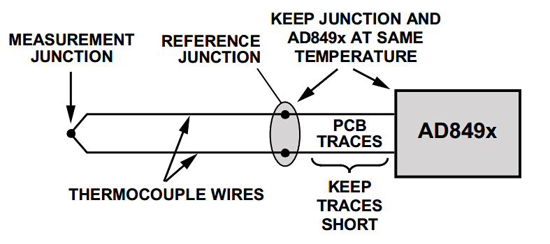
Figure 2. A diagram showing the junctions in the AD849x. Image used courtesy of Analog Devices
Thermocouple signal conditioners use an integrated temperature sensor for CJC. This temperature sensor actually measures the chip temperature rather than the cold junction of the thermocouple. Therefore, to more accurately measure the cold junction temperature, the signal conditioner should be near the cold junction. This shouldn’t be difficult, especially with signal conditioners such as the AD849x that come in a tiny 3.2 mm × 3.2 mm × 1.2 mm package.
Any temperature difference between the AD849x package and the cold junction appears as a temperature error at the final measured value. In addition to using short traces between the AD849x and the cold junction, it is also important to minimize the power consumption of the IC to avoid creating a temperature gradient across the PCB. This brings us to another important point about thermocouple signal conditioners: these devices typically draw only a small current from the power supply to minimize the self-heating effect. For example, the current consumption of the AD849x is 180 µA. If needed, the AD849x can deliver more than ±5 mA to a load; however, supplying large amounts of output currents can cause temperature gradients and introduce errors in our measurements.
The Nonlinearity Error of the AD849x
While thermocouples exhibit a nonlinear input-output characteristic, Equation 1 suggests that the output of the AD849x is a linear function of the hot junction temperature. It should be noted that the AD849x linearly amplifies the (cold junction compensated) thermocouple signal. Therefore, the amplified output is actually as nonlinear as the thermocouple signal. Therefore, the linear function given by Equation 1 only approximates the actual nonlinear response of the system.
Although the AD849x does not actively correct the thermocouple nonlinearity, it is designed based on a linear model of the sensor characteristic curve over the temperature range of interest. In other words, a straight line that “best-fits” the nonlinear characteristic of the supported sensor (link 200) is used to factory-calibrate the internal amplifier. This minimizes the nonlinearity error of the linear model provided by Equation 1. Within the specified temperature ranges, the values predicted by this equation should have a linearity error of less than ±2 °C. The following table gives the temperature ranges for each part of this family.
Table 1. Data used courtesy of Analog Devices
| AD849x ±2 °C Accuracy Temperature Ranges | ||||
| Part | Thermocouple type | Max Error | Ambient Temperature Range | Measurement Temperature Range |
| AD8494 | J | ±2 °C | 0 °C to 50 °C | -35 °C to +95 °C |
| AD8495 | K | ±2 °C | 0 °C to 50 °C | -25 °C to +400 °C |
| AD8496 | J | ±2 °C | 25 °C to 100 °C | +55 °C to +565 °C |
| AD8497 | K | ±2 °C | 25 °C to 100 °C | -25 °C to +295 °C |
Note that each device in this family is pre-trimmed to match the characteristics of J- or K-type thermocouples. This application note discusses algorithms that can significantly improve the linearity of the AD849x. Figure 3 shows the nonlinearity error of the AD8495 and that of a reference design with and without the correction algorithm.
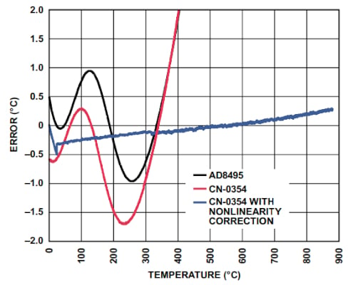
Figure 4. Nonlinearity error graph of the AD8495. Image used courtesy of Analog Devices
In this case, the linearity improvement algorithm reduces the error to less than ±0.5 °C.
AD849x Reference (REF) Pin Functionality
A thermocouple produces a negative voltage when its measurement (or hot) junction is at a temperature lower than its reference (or cold) junction. Therefore, if you need to measure negative temperatures, you should consider a signal conditioning circuit that can handle negative voltages. The obvious solution is to use an amplifier that runs off of dual supplies. The AD849x can address this issue even if the system is designed to run from a single supply. To do this, we can level-shift the output by applying an appropriate positive voltage to the reference pin (REF). In this case, the output will be lower than VREF when the measurement junction is at a negative temperature (Equation 1). The REF pin can also be useful when we need to level-shift the output to match the input range of the subsequent circuit in the signal chain.
Another Monolithic Thermocouple Example Solution—the LT1025
The LT1025 from Linear Technology is another monolithic solution for cold junction compensation. While the AD849x includes both an internal amplifier and a CJC circuit, the LT1025 only produces the cold junction compensation voltage. The functional block diagram of this IC is shown in Figure 5.
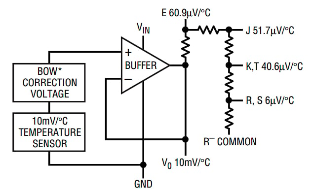
Figure 5. Block diagram for LT1025. Image used courtesy of Linear Technology
The device senses the package temperature and produces a 10 mV/°C buffered output. This voltage is then applied to a resistive voltage divider to produce outputs suitable for different types of thermocouples. As you can see, the LT1025 supports type E-, J-, K-, T-, R-, and S-type thermocouples. To learn about the theory behind analog CJC circuits, please refer to this article.
Exploring Thermocouple Applications With Example Amplifiers
Figure 6 shows how we can use the device to operate a K-type thermocouple.
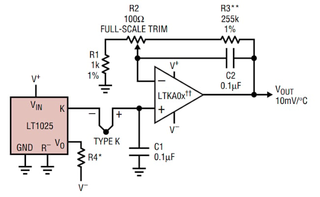
Figure 6. Diagram showing the operation of a K-type thermocouple. Image used courtesy of Linear Technology.
The LTKA0x is an amplifier specifically designed for thermocouple applications. It offers a low offset (< 35 µV) and drifts (<1.5 µV/°C). Besides, its bias current is also very low (<1 nA) which allows us to include filters with relatively large resistors (in the range of 10 to 100 kΩ) at the amplifier input without experiencing significant offset and drift effects.
Unlike the AD849x, the LT1025 solution separates the amplifier and cold junction compensation blocks. This helps to minimize the power dissipated by the CJC chip, which minimizes the self-heating effect. The LT1025 needs only 80 µA—much less than that of the AD849x which was 180 µA. Due to this small current consumption, the LT1025 experiences less than a 0.1 °C internal temperature rise for supply voltages under 10V.
Addressing Thermocouple Nonlinearity
If you’re familiar with CJC circuits, the theory behind the LT1025 should be relatively straightforward to you; however, another feature that deserves more explanation is the “Bow Correction Voltage” block. This block adds a nonlinear term to the 10 mV/°C voltage produced by the temperature sensor. This nonlinear term is added to address the thermocouple nonlinearity error in the CJC circuit. A basic CJC circuit attempts to fit a straight line to the thermocouple characteristic curve and uses this line of best fit to reproduce the thermocouple output over the cold junction temperature range. However, the output of the LT1025 consists of two different terms: a linear term proportional to temperature plus a quadratic term proportional to temperature deviation from 25 °C squared. Ideally, the LT1025 should implement the following equation:
\[V_{OUT}=aT+a\beta(T-25 °C)^{2}\]
Where:
- \(a\, and\,\beta\) are the coefficients for the linear and quadratic terms
- T denotes temperature
The value of \(\beta\) is chosen to reduce the nonlinearity error in all thermocouple outputs of the LT1025. Note that this quadratic term attempts to improve the thermocouple model used in the CJC circuit. In other words, it reduces the nonlinearity error of the CJC circuit but cannot compensate for the nonlinearity error of the thermocouple itself.
Now that you’re familiar with some of the important features of the AD849x and the LT1025, I recommend you take a look at the datasheet of these devices. There you’ll find additional details and various useful circuit diagrams for more specific use cases of these products.
To see a complete list of my articles, please visit this page.
Related Content