 Facebook
 Google
 GitHub
 Linkedin
Sampling, Amplifying, and Digitizing CCD Output Signals
In this article, we’ll see that the amount of noise in image data from a CCD sensor can be greatly reduced by a technique known as correlated double sampling.
Welcome to AAC's series on CCD (charge-coupled device) image sensors. Up to this point, we've covered the various types of CCDs, as well as their structure and operation and clock operations.
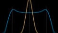
The previous article explained how a CCD output signal is generated, and it identified the three waveform features included in each pixel as the reset glitch, the reset level, and the data level.

I can’t help but marvel at the ingenuity of the human race when I consider that this lumpy, repetitive variation in voltage could somehow be transformed into a two-dimensional image that is comparable to, and in some ways superior to, our visual perception of reality. The capabilities of film are no less marvelous, but we can’t observe what’s happening in film at the molecular level in the way that we can look at a CCD waveform on an oscilloscope.
Correlated Double Sampling
When it comes to CCD signal processing, the most important topic is correlated double sampling (CDS). This term refers to a procedure in which a waveform is repeatedly sampled at two different moments, with each pair of samples being used to produce a single data point.
The benefit of correlated double sampling is noise reduction. You can think of it as a form of differential signaling: instead of subtracting one voltage signal from a complementary version of the same voltage signal, we temporally divide a single-ended waveform and subtract one instantaneous voltage from a second instantaneous voltage.
In the case of a CCD waveform, the two instantaneous voltages are acquired such that one captures the reference (AKA reset) level and the other captures the data level:

Noise Reduction
As with differential signaling, correlated double sampling is a powerful means of reducing noise, because any noise source that affects both the reference level and the data level will be eliminated when one voltage is subtracted from the other.
A major noise source in a CCD signal is called kTC noise, which is thermal noise associated with capacitance. The kTC noise magnitude is the same during the reference and data portions of a given pixel, and consequently it is eliminated by correlated double sampling.
In general, the efficacy with which CDS attenuates noise sources depends on bandwidth—in other words, it depends on how quickly the noise signal is changing. There is a certain period of time that separates the first sample from the second sample, and if the value of the noise signal changes significantly during this period, the noise isn’t removed by subtraction.
CCDs generate higher-frequency noise that correlated double sampling cannot eliminate, but the technique reduces the effect of lower-frequency noise such as flicker (AKA 1/f) noise, slow power supply variations, and thermal drift.
Implementing Correlated Double Sampling
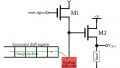
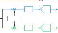
The term “sampling” might make you think of analog-to-digital conversion, as if CDS is achieved by taking two ADC samples. However, CCD systems perform this double sampling in the analog realm. There are various circuit realizations; the one shown below is straightforward and helps to illustrate the general concept.

The circuit consists of two sample-and-hold (S/H) blocks and a difference amplifier. The sample-and-hold operation captures the voltage level of a signal at one specific moment in time and then maintains that value.
A basic S/H solution is just a capacitor with a FET that separates the capacitor from the input signal:

A sample-control pulse switches on the FET and allows the capacitor to charge up to the input voltage. As long as the other capacitor terminal is connected to a high-impedance node, no significant discharge can occur, and consequently the voltage on the capacitor stays (almost) constant long enough to perform whatever other signal-processing tasks are required.
Higher performance (or at least reduced design effort) can be achieved by incorporating a dedicated sample-and-hold IC. Some examples are the LFx98x series from Texas Instruments, the SMP04 from Analog Devices, and the DS1843 from Maxim.
In the CDS circuit, one S/H block is triggered at treference (i.e., at some instant during the reference-level portion of the pixel waveform), and the other is triggered at tdata (i.e., at some instant during the data-level portion). The difference amplifier then subtracts the data level from the reference level and produces a single output voltage that is ready for further processing.
CCD Signal Processors
There are various other aspects of CCD analog signal processing and A/D conversion, but I don’t think that they merit detailed discussion—honestly, few if any of us will ever need to create a customized CCD interface from a collection of discrete ICs. Highly integrated solutions are available, and they offer convenience and performance that can’t be beat.
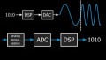
We’ll conclude this article with brief descriptions of other portions of the CCD signal chain, with a little help from the datasheet for the AD9845B, a CCD signal processor from Analog Devices.

Diagram taken from the AD9845B datasheet.
- The DC offset is shifted by first AC coupling the signal then applying a DC restore voltage.
- The signal is amplified in accordance with the full-scale range of the ADC.
- The optical-black-clamp subcircuit uses information from light-shielded pixels to improve dynamic range by removing an offset caused by dark current.
- Properly synchronized analog-to-digital conversion produces numerical pixel data, with ADC resolution chosen according to the maximum dynamic range of the CCD.
Conclusion
We explored correlated double sampling, and we took a high-level look at a typical CCD signal-processing system. The next article will continue the Image Sensor Technology series with an interesting CCD topic that is relevant to specialized applications.
Related Content


How sensitive is the temporal correlation signal to variations in phase of the signal?
Did I read the circuit correctly? They let the optical black clamp circuit inject a coarse grained 8 bit signal to mix with the 12 bit ADC signal?
Do you ever use real data with any of your articles?
Thank you for explaining what they did in this AD9845B. It looked interesting, but now I know how they are fiddling with the basic signal, I know it is basically worthless to me since the dark noise, flicker, and other noises are my main interest. I don’t know how to “build my own”, but you have made it clear that an off the shelf chip, meant for mass markets, is not going to cut the mustard. Too bad this is a one way discussion. But I often write things to clarify for myself, since organizations seldom listen. You must get tired of writing sometimes. The web is full of this stuff. How does anything ever get done?
You said “few if any of us will ever need to create a customized CCD interface from a collection of discrete ICs” so it is possible to build one’s own interface to the sensor, and not rely one someone else who might not care as much about the many parts of the noise signals?