 Facebook
 Google
 GitHub
 Linkedin
Intro Software Walkthrough: Fast Fourier Transforms and the Xilinx FFT IP Core
This article will explain some of the most important settings and design parameters for the Xilinx FFT IP core and function as a basic walkthrough of the Fast Fourier Transform interface.
This article will explain some of the most important settings and design parameters for the Xilinx FFT IP core and function as a basic walkthrough of the Fast Fourier Transform interface.
The Fast Fourier Transform (FFT) refers to a class of algorithms that can efficiently calculate the Discrete Fourier Transform (DFT) of a sequence. The DFT is a powerful tool in the analysis and design of digital signal processing systems and, consequently, the FFT is a commonly used transform in a wide range of DSP applications.
The FFT has a rather complicated algorithm and its hardware implementation can be a challenge. That’s why different FPGA vendors have provided customizable FFT IP cores that can be added to a design with just a few clicks. However, the designer still needs to know some details about the FFT hardware implementation before being able to use these IP cores with confidence. There are many FFT IP cores to choose from. Intel has its own FFT IP Core, as does Lattice Semiconductor, and engineering firms such as Dillon Engineering. In this article, we will look at the FFT IP core provided by Xilinx.
For a general discussion about integrating a Xilinx IP core into your design, please see this article on the Xilinx CORDIC Core. This article will explain some of the important implementation parameters for the Xilinx FFT IP core, including what each of these settings accomplishes for the engineer.
Adding the FFT Core
To add the FFT core to your ISE project, click on “New Source” under the “Project” tab and choose “IP (CORE Generator & Architecture Wizard)”. After giving your new source a name and location, you can find the FFT core by choosing “FFTs” from the “Digital Signal Processing” category, as shown in Figure 1.
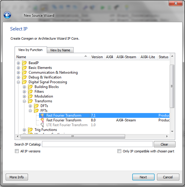
Figure 1
Then, a GUI will open which allows you to customize the core according to your needs.
Choosing the Core Parameters: Page 1
The first page of the core settings is shown in Figure 2.
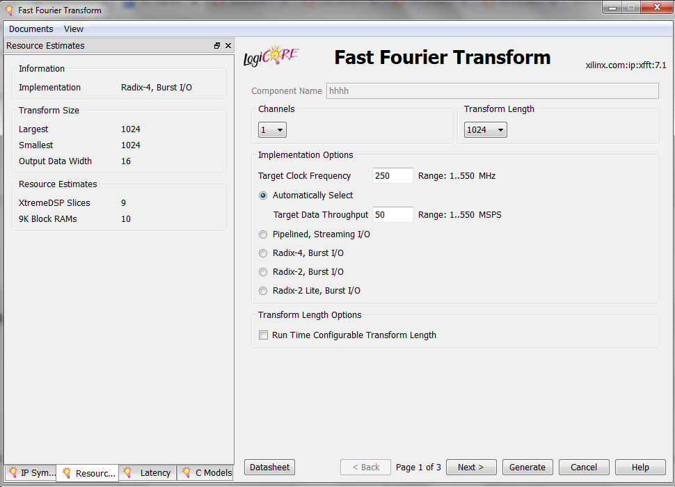
Figure 2
At the top of the page, we can choose the number of channels for this core. This is useful when we need to calculate the FFT of several different signals. If all of these FFTs have exactly the same parameters, we can use one multi-channel FFT block instead of instantiating a single-channel FFT core several times in our HDL code. With a multi-channel implementation, some hardware sharing can be done by the synthesis tool and we can have a more efficient design.
The core supports up to 12 channels. If a multi-channel core is chosen, some of the core ports, such as the FFT input and output ports, will be duplicated to accommodate working on multiple signals simultaneously. You can check the added ports by clicking on the “IP Symbol” tab in the core GUI (you can see this tab in the bottom-left corner of Figure 2). Note that multi-channel operation is not supported when the core’s “Implementation Options” is set to “Pipelined, Streaming I/O” (see Figure 2).
The “Transform Length” specifies the length of the FFT transform. Its maximum value is 65536.
Implementation Options
Next, we reach the “Implementation Options”. As shown in Figure 2, there are five different options for the core implementation. The first option is “Automatically Select”. In this case, the software chooses the smallest implementation that meets the specified “Target Data Throughput” for a given “Target Clock Frequency”.
Note that the “Target Clock Frequency” and the “Target Data Throughput” are only used to automatically select an implementation and calculate the design latency. You can connect a clock of any frequency to the clock input of the implemented FFT core. However, you will get a different latency, if the actual clock frequency is different from the one you specify in the core GUI. (Please visit this forum post page for more information.)
As shown in the figure, the other four implementation options are:
- Pipelined, Streaming I/O
- Radix-4, Burst I/O
- Radix-2, Burst I/O
- Radix-2 Lite, Burst I/O
These options offer a trade-off between the core size and the throughput. This trade-off is depicted in Figure 3. As a rule of thumb, the core size increases by a factor of two from one architecture to the next one in the figure.
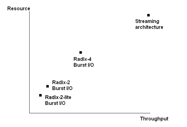
Figure 3. Image courtesy of Xilinx.
The “Pipelined, Streaming I/O” implementation processes data continuously. With this implementation, we can simultaneously process the current frame of data, load the data for the next data frame, and unload the results of the previous data frame. However, with “Radix-4, Burst I/O”, “Radix-2, Burst I/O”, and “Radix-2 Lite, Burst I/O”, the transform calculation and the data I/O cannot occur simultaneously.
For these three implementations, we have to first load a data frame, calculate the transform, and then unload the result. Unloading the result of the current frame can be simultaneous with loading the new data frame only if the data is unloaded in a particular order called “bit/digit-reversed order”.
What Is Bit/Digit-Reversed Order?
From the implementation point of view, it is easier to generate the output of the FFT algorithm in a particular order called bit/digit-reversed order.
As an example, consider a radix-2 eight-point FFT block that sequentially receives eight time-domain data samples and then sequentially produces the FFT output values. We can apply the input samples in the normal order, i.e., we first apply x[0], then x[1], then x[2], and so on; however, the FFT core may be designed to generate the output samples with the order X[0], X[4], X[2], X[6], X[1], X[5], X[3], and X[7]. In this case, the binary equivalent of the index of the generated output samples is 000, 100, 010, 110, …. These correspond to the bit-reversed, or “mirrored,” versions of the normal indices (e.g., 000 becomes 000, 001 becomes 100, 010 becomes 010, 011 becomes 110, etc.).
That’s why we say that the output is in bit-reversed order. To see an example of the digit-reversed indices that a radix-4 FFT may generate, refer to page 6 of the Xilinx FFT core datasheet.
Generating the FFT outputs in bit/digit-reversed order not only makes the memory usage of the design more efficient but also significantly simplifies the design. However, these advantages are achieved at the cost of having to produce the FFT output in bit/digit reversed order. In this case, we'll have to reorganize the FFT output data somewhere in our calculations to remove the effects of bit/digit-reversed order. Refer to Section 9.2 of the book Discrete Time Signal Processing for more details. Note that the implementation simplifications can be achieved by making either the input or the output of the FFT bit/digit reversed; however, the Xilinx FFT core always receives the input in the normal order.
The Xilinx FFT core output can be either in bit/digit-reversed order or in natural order. When natural order output is selected, either additional memory resources will be utilized or a time penalty will be imposed, depending on which core implementation is selected.
The last option of page 1 is the “Run Time Configurable Transform Length”. Checking this option will make the FFT length runtime configurable. In this case, two new input ports, i.e., NFFT and NFFT_WE, will be added to the “IP Symbol”. The NFFT is the input that specifies the transform length at runtime, and NFFT_WE is the active-high write enable for the NFFT input. We are allowed to apply any value less than or equal to the “Transform Length” that was chosen at the top of page 1 of the core GUI. For example, a 1024-point FFT block will be able to compute transforms of lengths 1024, 512, 256, and so on. Choosing this option can increase the core size and reduce its maximum clock frequency.
Choosing the Core Parameters: Page 2
The second page of the core settings is shown in Figure 4.
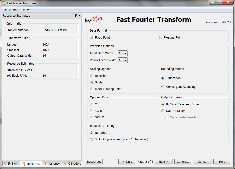
Figure 4
In the “Data Format” section, we can specify the input and output data format, which can be either “Fixed Point” or IEEE-754 single-precision “Floating Point”. In the multi-channel mode of operation, the floating point format is not supported.
The next section specifies the number of bits used to represent the “Input Data” and the “Phase Factor”. The “Phase Factor” refers to the constant trigonometric coefficients that are multiplied by the data samples in the course of the algorithm. As you can see, the “Input Data Width” and the “Phase Factor Width” can be chosen independently.
Next, let’s look at the “Scaling Options” section, which is related to bit growth arising from the arithmetic operations performed in the course of the algorithm. To gain some insight into this issue, consider the signal flow graph of a radix-2 decimation-in-time eight-point FFT algorithm, as shown in Figure 5.
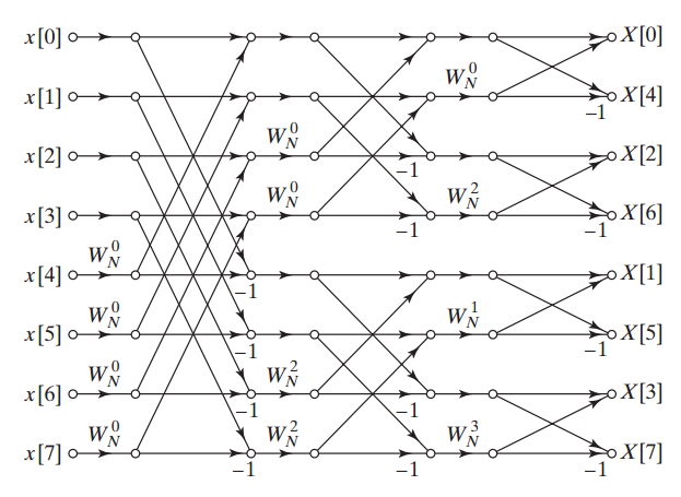
Figure 5. The signal flow graph of a radix-2 eight-point FFT. Image courtesy of Discrete Time Signal Processing.
We can decompose this signal flow graph into small units called a “Butterfly,” as shown in Figure 6.
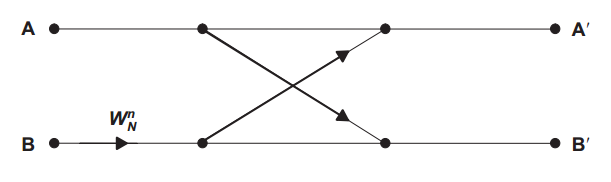
Figure 6. A radix-2 decimation-in-time butterfly. Image courtesy of TI.
The different parts of the signal flow graph in Figure 5 use the above butterfly with different phase factors, $$W_{N}^{n}$$. The value of $$A^{'}$$ and $$B^{'}$$ can be found from the following equations:
$$A^{'} = A + W_{N}^{n} B$$
$$B^{'} = A - W_{N}^{n} B$$
The parameters in these two equations all can have complex values. Hence, these two complex-valued equations will lead to four real-valued equations. It can be shown that either the real or imaginary part of $$A^{'}$$ or $$B^{'}$$ will grow by a factor of $$1+ \sqrt{2} \approx 2.414$$ relative to the real or imaginary part of $$A$$ or $$B$$ i.e., the butterfly input signals. (See this TI application report for more information.) Considering the growth factor of 2.414 for a radix-2 butterfly, we have to increase the width of the registers storing $$A^{'}$$ and $$B^{'}$$ by two bits compared to the width of the registers used for $$A$$ and $$B$$, otherwise overflow can occur, resulting in invalid calculations.
Scaling Options
The “Scaling Options” section of the FFT core GUI provides different ways to deal with the problem of overflow. We’ll briefly look at the supported options:
Unscaled
By choosing the “Unscaled” option, the width of the registers will be chosen long enough to avoid overflow. This can use more FPGA resources in comparison with the “Scaled” option that will be discussed next. As mentioned above, a single radix-2 butterfly requires a maximum bit growth of up to two bits to avoid overflow. However, not all of the FFT butterflies will experience this maximum bit growth. In fact, to perform full-precision unscaled arithmetic without overflow, the Xilinx FFT IP core chooses the integer part of the FFT output such that it is equal to (integer width of the input + $$log_2(transform \; length)$$ + 1) . For example, assume that we have a 1024-point unscaled FFT core with 16-bit inputs, where 3 bits are allocated for the integer part and 13 bits for the fractional part. In this case, the integer part of the output will have 3+10+1=14 bits. The software will make the width of the fractional part of the output equal to that of the input. Hence, the FFT output will have a total of 14+13=27 bits. Note that the integer width is chosen to avoid overflow but the fractional width is chosen based on the acceptable quantization error. Most of the IP cores truncate the fractional part of the computations to reach a fractional width equal to that of the core input.
Scaled
If we choose the “Scaled” option, we can apply a user-defined scaling schedule to the core calculations. In this case, the result of the different stages of the algorithm will be divided (or right-shifted) by the user-defined scaling values so that overflow does not occur. For example, assume that we have a 1024-point FFT block implemented using the “Radix-2, Burst I/O” structure. For this example, we have $$log_2(point \; size) = log_2(1024)=10$$ radix-2 stages. Therefore, we’ll need to give the core 10 scaling values to control overflow. According to the Xilinx FFT core datasheet, we can use [01 01 01 01 01 01 01 01 01 10] as a conservative scaling schedule for this particular example. This scaling schedule translates to a right shift by 2 for stage 0 of the algorithm and a right shift by 1 for the nine remaining stages. In other words, the two LSB bits give the scaling value for stage 0, the next two bits give the scaling value for stage 1, and so on. These scaling values can be applied to the scaling schedule input for the core, i.e., SCALE_SCH, which becomes active when the “Scaled” option is selected. Note that, with a given input type, it can be difficult to find the minimum scaling value for each FFT stage that prevents from overflow. That’s why Xilinx has developed a C model that can be used to find an appropriate scaling schedule for a given fluctuation level in the input signal. Refer to page 21 of the FFT core datasheet for more information about using this C model.
Block Floating Point
“Block Floating Point” is the next option for avoiding the overflow problem. When the FFT input is not well understood and can exhibit large fluctuations, a “Scaled” structure may not be successful. In such cases, “Block Floating Point” can be used. This option prevents overflow by allowing the core to determine the appropriate scaling value for the different stages of the algorithm. The amount of scaling utilized will be reported as a block exponent by the BLK_EXP output of the core. “Block Floating Point” mode may require significantly more resources compared to an implementation that uses “Scaled” mode.
For more information about the effect of finite register length on FFT performance, please refer to Section 9.7 of Discrete Time Signal Processing.
Rounding Modes
The “Rounding Modes” in page 2 of the core GUI specifies the technique used to reduce the fractional width of the butterfly computations. There are two options: “Truncation” and “Convergent Rounding”. The “Truncation” method is simpler and uses fewer hardware resources; however, “Convergent Rounding” avoids the DC bias introduced by “Truncation”.
Optional Pins
The “Optional Pins” section allows us to add some optional pins, such as Clock Enable (CE) and Synchronous Clear (SCLR), to the core.
Output Ordering
The “Output Ordering” option specifies whether the output will be generated in “Natural Order” or “Bit/Digit Reversed Order”.
Input Data Timing
“Input Data Timing” is an option included to make the core compatible with its earlier versions. For a new design, you can choose “No Offset”.
Choosing the Core Parameters: Page 3
Page 3 of the settings is shown in Figure 7.
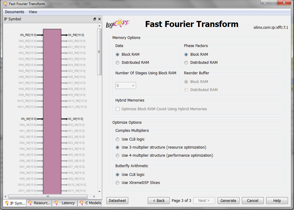
Figure 7
This last page of the settings specifies some implementation options. We can guide the core to use the FPGA resources, such as the Block RAMs, Distributed RAMs, or DSP slices, according to our project’s requirements. Since these options are fairly straightforward, we won’t go through the details. Please refer to the core datasheet to learn about using these options correctly.
After specifying all these parameters, we can generate the core and add it to our design. Now that you have some insight into the different options of the Xilinx FFT core, you should be able to more easily grasp the material covered in the core datasheet. Remember that you’ll need to carefully investigate the core timing diagrams before you can use it correctly in your design!
To see a complete list of my articles, please visit this page.


Thanks for this article. It gave me a quick insight to the Xilinx FFT IP. If you can upgrade it for the new version it will be great.
Thanks, that helped me a lot : ) it will very helpful also if you’ll add simulation data in this article or write another article about it : )
Thank you for a very informative and a well-summarized introduction about the Xilinx FFT IP!