Facebook
 Google
 GitHub
 Linkedin
Peak Detectors
Peak detectors tend to be a bit tricky. A surprising number of the schemes using an op amp and a diode tend toward oscillation or other misbehavior.
When you analyze the feedback loop in Figure 18-10, you find that the diode and the capacitor at the output place an unusual burden on the op amp. When the signal moves up (for a positive peak detector) the output is connected to a large capacitance. When the signal moves down, there is no load at all.
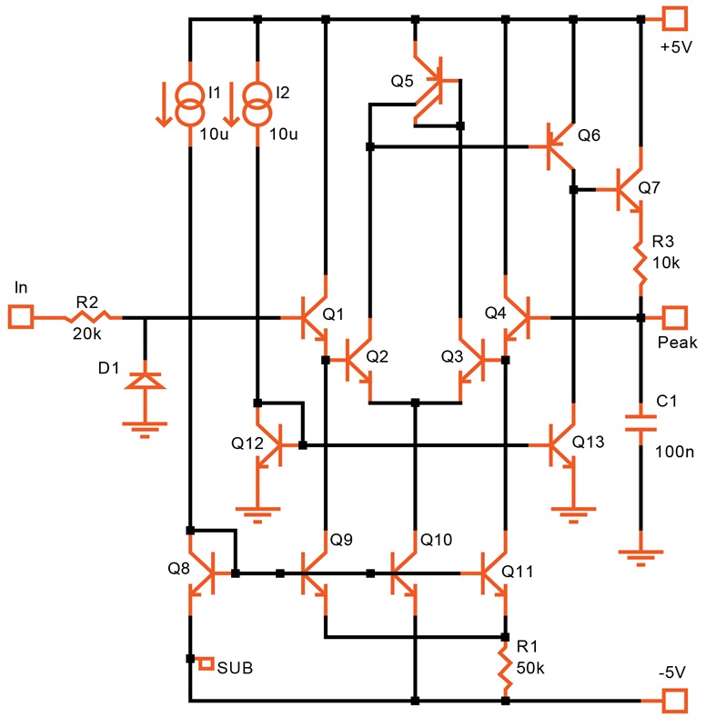
Figure 18-10. [click to enlarge] Peak detector with differential NPN Darlington pair.
This circuit uses a bipolar Darlington pair to provide a high-impedance input at the (external) capacitor. For operation over a wide temperature range, the outer transistors (Q1, Q4) are biased at about 0.8 μA by Q9 and Q11. The output impedance of the op amp is artificially enlarged by R3 to provide frequency compensation (together with C1).
A Fundamental Question
There is a fundamental question to every peak detector: How long should the voltage stay on the capacitor? If the answer is "forever," then the detector displays the highest peak for an infinite history of input signals. This is probably not what you want.
For any other answer, you have two choices:
- Discharge C1 slowly, so the voltage stays within the desired accuracy over the time of interest.
- Reset C1 before each measurement.
In the circuit of Figure 18-10, the capacitor is discharged by the base current of Q4. This current amounts to about 5 nA. If the peak voltage is 1 V, you lose about 1% in 200 ms with 100 nF of capacitance. The discharge current varies from chip to chip and with temperature.
A Single-Supply Peak Detector
Figure 18-11 shows a peak detector that operates from a single supply voltage.
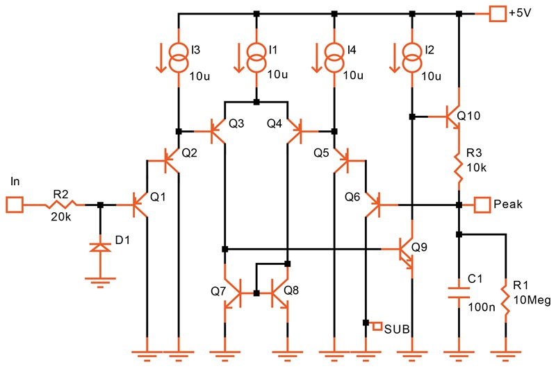
Figure 18-11. Single-supply peak detector with a lower input current.
The Darlington input pair of the op amp is more elaborate, and the operating currents of the outer transistors (Q1, Q6) are merely the base currents of the inner ones. This limits the temperature range to about 100 °C, but it also lowers the input current.
Notice the discharge resistor R1. Without it, the base current of Q6 would charge C1 (it flows out of the base). Thus, in this circuit, a controlled rate of discharge through R1 is essential.
In both examples, the supply voltage must be lower than the emitter-base breakdown voltage of the output transistor. If it needs to be higher, use an additional diode in series with the emitter.
CMOS Peak Detectors
CMOS devices are much better suited for peak detector design than bipolar ones. There are two reasons for this, the first of which is that there is no DC input current.
The second reason is that you can reset a capacitor to 0 V. The collector-emitter voltage of a bipolar transistor, on the other hand, does not go to zero. There is always a remaining voltage of about 100 or 150 mV.
An example of a CMOS peak detector is shown in Figure 18-12. As in the bipolar examples, the feedback loop is compensated by Cext and the resistor in the output path (R1).
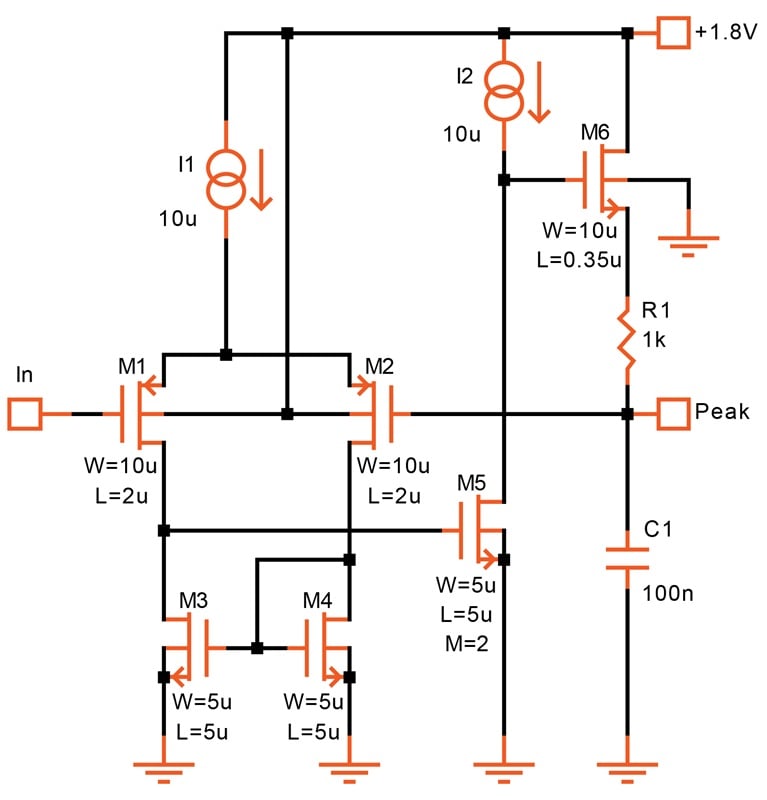
Figure 18-12. [click to enlarge] CMOS peak detector.
Since there is no input current, C1 can be made quite small, to the point where it can be internal. However, be aware that the smaller C1 is, the more difficult it becomes to compensate the feedback loop.